 | –≠–ª–µ–∫—Ç—Ä–æ–Ω–Ω—ã–π –∫–æ–º–ø–æ–Ω–µ–Ω—Ç: HBCR-1810 | –°–∫–∞—á–∞—Ç—å:  PDF PDF  ZIP ZIP |
Programmable Bar Code Decode ICs
Technical Data
Features
∑ Ideal for Hand Scanning and
Many Automated Scanning
Applications
∑ Supports Code 39, UPC /
EAN / JAN and Interleaved 2
of 5 Standard Bar Code
Symbologies
∑ Automatic Code Recognition
∑ Choice of Parallel or Serial
Interface
∑ Full Duplex ASCII Interface
∑ Extensive Configuration
Control
∑ Low Current CMOS
Technology
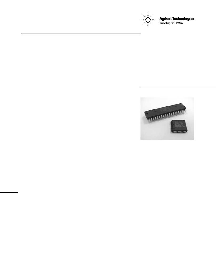
∑ 40 Pin DIP and 44 Pin PLCC
Packages
∑ Audio and Visual Feedback
Control
∑ Single +5 Volt Supply
Description
Agilent's Bar Code Decoder ICs
offer flexible bar code decoding
capability that is designed to
give OEMs the ability to address
a large number of industry
segments and applications.
Flexibility is made possible
through sophisticated firmware,
which allows the ICs to accept
data from a wide variety of
scanners and to automatically
recognize and decode the most
popular bar code symbologies.
User implementation of the
decoder ICs is easy since it
requires only a few supporting
chips and components and
provides a standard I/O interface.
Manufacturers of data collection
terminals, point of sale terminals,
keyboards, weighing scales, and
other data collection and material
handling equipment are finding a
growing demand for bar code
reading capability in their
products. The HBCR-1810 series
decoder ICs make it easy to add
this capability without the need to
invest in the development of bar
code decoding software.
The bar code decoder ICs are
compatible with most hand held
scanners. The HBCR-1810 series
HBCR-1810
HBCR-1811
is compatible with fixed beam
non-contact scanners, digital
wands, and digital slot readers.
The decoder ICs decode the bar
code symbologies now in use for
most applications in the
industrial, retail, government, and
medical market. The ICs support
Code 39 (Standard or Extended),
Interleaved 2 of 5, and the UPC/
EAN/JAN Codes. Whenever more
than one symbology is enabled,
the bar code being scanned will
automatically be recognized and
decoded, except for Standard and
Extended Code 39 which are
mutually exclusive. Bi-directional
scanning is allowed for all bar
codes except UPC/EAN/JAN with
supplemental digits, which must
be scanned with the supplemental
digits last.

2
2
The I/O for the decoder ICs is full
duplex, 7 bit ASCII. Both serial
and parallel interfaces are
available. The serial interface can
be converted to an RS232C
interface or connected directly to
another microprocessor for data
processing. The parallel interface
can be connected to a tri-level
bus through a 74LS245 or
equivalent. Feedback to the
operator is accomplished by
signals for an LED and a beeper.
In addition, there are
programmable functions covering
items such as code selection and
beeper tone.
The ICs are CMOS, in either a 40
pin DIP package or a 44 pin
PLCC package. All ICs require a
dedicated external data memory,
2K or 8K x 8 bit static RAM (only
1K is needed) and address latch
chip (a 74LS373 or equivalent).
The crystal frequency is 12.000
MHz.
Performance Features
Bar Codes Supported
The decoder IC is capable of
reading popular bar code
symbologies: Code 39 (Standard
or Extended), Interleaved 2 of 5,
and UPC/EAN/JAN.
Code 39 is an alphanumeric code,
and Extended Code 39 encodes
the full 128 ASCII character set
by pairing Code 39 characters.
Both can be read bi-directionally
with message lengths of up to 32
characters. An optional checksum
character can be used with these
codes, and the ICs can be
configured to verify this
character prior to data
transmission. Note that enabling
Extended Code 39 will disable
Code 39 since they are mutually
exclusive.
Interleaved 2 of 5 code, a
compact numeric only bar code,
can also be read bi-directionally
with message lengths from 4 to
32 characters. To enhance data
accuracy, optional checksum
character verification and/or
message length checking can be
enabled.
The following versions of the
UPC, EAN and JAN bar codes can
be read bi-directionally: UPC-A,
UPC-E, EAN-8, EAN-13, JAN-8,
and JAN-13. All versions can be
enabled simultaneously or
decoding can be restricted to
only the UPC codes.
UPC, EAN, and JAN codes
printed with complementary two
digit or five digit supplemental
encodations can be read in two
different ways. If the codes are
enabled without the supplemental
encodations, then only the main
part of symbols printed with
supplemental encodations will be
read. If the reading of
supplemental encodations is
enabled, then only symbols with
these supplements will be read.
Whenever supplemental
encodations are enabled, the bar
code symbols must be read in the
direction that results in the
supplements being scanned last.
Scanner Input
The decoder ICs are designed to
accept data from hand held
digital scanners or slot readers
with the following logic state:
black = high, white = low.
Scanner input can be disabled by
software command. This allows
an application program to control
when an operator can enter data,
preventing inadvertent data entry.
It also allows the program to
verify each scan before enabling
subsequent scans.
Data Communications
The serial port supports a wide
range of baud rates, parities, stop
bits, and terminator characters,
as described in Summary of
Features and Configuration
Control table. Software control
of data transmission is
accomplished with an Xon/Xoff
(DC1/DC3) handshake.
The parallel port data has odd
parity. The default terminator
character is a CR, but it can be
changed by software commands.
An Xon/Xoff (DC1/DC3) software
handshake is available to control
data transmission.
Feedback Features
Both audio and visual feedbacks
are possible with the decoder ICs.
In both cases, the outputs from
the ICs must be buffered before
driving the actual feedback
mechanism. An LED or beeper
connected to the decoder ICs can
be controlled directly by the IC,
with signals generated by
successful decodes or can be
controlled by the host system.
3
In addition, the tone of the
beeper can be varied by software
commands to be one of 16
different frequencies, or can be
silenced.
Power Requirements
The decoder IC operates from a
+5 volt DC power supply. The
maximum current draw is 19mA.
The maximum power supply
ripple voltage should be less than
100 mV, peak-to-peak.
Configuration Control
Configuration of the decoder IC
is determined by hardwire
connections and/or through
software commands. Hardwire
selection is limited to key
operating parameters.
A greater range of configuration
control is available via software
commands. A summary of the
decoder IC features and
configuration control is
presented in Summary of
Features and Configuration
Control table.
Handling Precautions
The decoder ICs are extremely
sensitive to electrostatic
discharge (ESD). It is important
that proper anti-static procedures
be observed when handling the
ICs. The package should not be
opened except in a static free
environment.
Manuals
The decode IC Users Manual
covers the following topics:
∑ Data output formats
∑ I/O interfaces
∑ Laser input timing diagrams
∑ Escape sequence syntax and
functionality
∑ Example schematics
∑ All configurable options
∑ Bar code menus
∑ Scanner positioning and tilt
∑ Sample bar code symbols
∑ Appendices describing bar code
symbologies
Part Number
Description
HBCR-1810
CMOS, 40 pin DIP, bulk ship, no manuals
HBCR-1811
CMOS, 44 pin PLCC, bulk ship, no manuals
Option A01
IC individually boxed with manuals
HBCR-1997
Series 1810 manuals
Ordering Information
4
4
Recommended Operating Conditions
Parameter
Symbol
Minimum
Maximum
Units
Notes
Supply Voltage
V
CC
4.0
6.0
V
1
Ambient Temperature
T
A
- 40
+ 85
∞
C
Crystal Frequency
XTAL
0 (DC)
12.000
MHz
2
Element Time Interval
ETI
150
70 000
µ
s
3
Notes:
1. Maximum power supply ripple of 100 mV peak-to-peak.
2. The HBCR-1810 series uses a 12.000 MHz crystal. For different crystal frequencies, multiply the specified baud rate and beeper
frequencies by (crystal frequency/12.000 MHz) and multiply the element time interval ranges by (12.000 MHz/crystal frequency).
3. At the specified crystal frequency.
Absolute Maximum Ratings
Parameter
Symbol
Minimum
Maximum
Units
Notes
Storage Temperature
T
S
- 55
+ 150
∞
C
Supply Voltage
V
CC
- 0.5
+ 7.0
V
1
Pin Voltage
V
IN
- 0.5
V
CC
+ 0.5
V
1, 2
Notes:
1. Voltage on any pin with respect to ground.
2. T
A
= 25
∞
C.
DC Characteristics
(T
A
= - 40
∞
C to +85
∞
C, V
CC
= 4.5 V to 5.5 V, V
SS
= 0 V)
Test
Symbol
Parameter
1810 Pins
1811 Pins
Min.
Max.
Units
Conditions
V
IL
Input Low Voltage
All
All
-0.5
0.2 V
CC
≠ 0.1
V
V
IH
Input High Voltage
except 9,18
except 10, 20
0.2 V
CC
+0.9
V
CC
+ 0.5
V
V
IH1
Input High Voltage
9, 18
10, 20
0.7 V
CC
V
CC
+ 0.5
V
V
OL
Output Low Voltage
1-8, 10-17,
2-9, 11, 13-19,
0.45
V
I
OL
= 1.6 mA
21-28
24-31
V
OL1
Output Low Voltage
30,32-39
33, 36-43
0.45
V
I
OL
= 3.2 mA
V
OH
Output High Voltage
1-8, 10-17,
2-9, 11, 13-19,
2.4
V
I
OH
= -60
µ
A
21-28
24-31
0.75 V
CC
V
I
OH
= -30
µ
A
0.9 V
CC
V
I
OH
= -10
µ
A
V
OH
Output High Voltage
30, 32-39
33, 36-43
2.4
V
I
OH
= -400
µ
A
0.75 V
CC
V
I
OH
= -150
µ
A
0.9 V
CC
V
I
OH
= -40
µ
A
I
IL
Input Low Current
1-8, 10-17,
2-9, 11, 13-19,
-10
-200
µ
A
V
IN
= 0.45 V
21-28
24-31
I
IL2
Input Low Current
18
20
-3.2
mA
V
IN
= 0.45 V
I
IL1
Input Leakage Current
32-39
36-43
±
10
µ
A
0.45
V
IN
V
CC
R
RST
Pulldown Resistor
9
10
20
125
K
I
CC
Power Supply Current
-
-
18
mA
All outputs
disconnected
5
Summary of Features and Configuration Control
Hardwire/
Software
Feature
Function or Value
Control
[1]
Default Setting
[2]
Mode
[3]
Notes
Mode of Operation
Parallel or Serial Mode
Hardwire
Parallel
N/A
Baud Rate
300, 1200, 2400, 9600
Hardwire
300 Baud
Serial
Parity
0s, 1s, Odd, Even
Hardwire
0s
Serial
4
Stop Bits
1 or 2
Hardwire
2
Serial
Terminator
C
R
, C
R
L
F
, H
T
, None
Hardwire
C
R
Serial
Character
User defined
Software
C
R
Both
5
(10 characters max.)
Header Character
User defined
Software
No header
Both
(10 characters max.)
character
Data Output Character
X
ON
/X
OFF
(DC1/DC3)
Software
No pacing
Both
Code 39
Software
Industrial Code
Interleaved 2 of 5
Code 39
Select
Extended Code 39
Both
Interleaved 2 of 5 code
UPC/EAN/JAN together;
Software
UPC/EAN/JAN codes
Both
Or UPC only
UPC/EAN/JAN
Enable 2 or 5 Digit
Software
Supplements not
Code Select
supplements
enabled
Suppress Zeros UPC-E
Software
Zeros included
Checksum Verification
Code 39 checksum
Both
No Checksum
Enable
Interleaved 2 of 5 checksum
Software
Verification
Both
Interleaved 2 of 5
User defined up to 32
Software
Variable Length
Both
Label Length Check
characters or variable length
Scanner Disable
Disables scanner input
Software
Input Enabled
Both
Good Read Beep
Enables good read beep in
Software
Beep signal enabled;
Both
Select
one of 16 tones
tone = 15
Sound Tone
Command to sound tones
Software
N/A
Both
Defines one of 16 tones
LED Control
Controls LED driver circuit
Software
LED to flash upon
Both
good read
Status Request
Gives status of decoder
Software
N/A
Both
IC configuration
Hard Reset
Resets decoder IC to
Software
N/A
Both
hardwire configuration and
default software settings
Notes:
1. Software commands are sent by means of escape sequences.
2. Default settings are those settings which result when the relevant pins have been tied to +5 V and no software commands have
been sent to the decoder IC.
3. Some functions apply only when the decoder IC is operating in the serial mode. Others apply in both the parallel and serial modes.
4. In parallel mode, the parity is always odd.
5. In the parallel mode, the terminator character is C
R
unless changed through software commands.
6
6
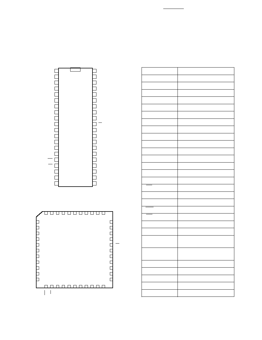
HBCR-1810 Series -- Serial Pinout
Mnemonic
Description
BRO
Baud Rate Select 0
BR1
Baud Rate Select 1
SB
Stop Bits
PT0
Parity Select 0
PT1
Parity Select 1
TR0
Trailer Select 0
TR1
Trailer Select 1
RxD
Received Data
TxD
Transmitted Data
LED
LED Control
BPR
Beeper Control
RST
Reset
SI
Scanner Input
SZ
Suppress Zeroes, UPC-E
NC
No Connect
EA
Connect to +5 V
ALE
Address Latch Enable
MDE
Mode
WR
Memory Write
RD
Memory Read
XTAL 1
Crystal Input 1
XTAL 2
Crystal Input 2
C39FLA
Code 39 Full ASCII
Conversion
C39CSE
Code 39 Check Character
Enable
AD0-AD7
Address/Data Bits 0-7
A8
Memory Address Line 8
A9
Memory Address Line 9
V
SS
Ground
V
CC
+5 V Power
BR0
BR1
SB
PT0
PT1
TR0
TR1
SZ
RST
RxD
TxD
SI
NC
LED
BPR
WR
RD
XTAL 2
XTAL 1
VSS
VCC
AD0
AD1
AD2
AD3
AD4
AD5
AD6
AD7
EA
ALE
NC
MDE ≠ 0 V
C39FLA
C39CSE
NC
NC
NC
A9
A8
1
2
3
4
5
6
7
8
9
10
11
12
13
14
15
16
17
18
19
20
40
39
38
37
36
35
34
33
32
31
30
29
28
27
26
25
24
23
22
21
1810
TR0
1811
6
5
4
3
2
1
44
43
42
41
40
TR1
SZ
RST
RxD
NC
TxD
SI
NC
LED
BPR
39
38
37
36
35
34
33
32
31
30
29
7
8
9
10
11
12
13
14
15
16
17
AD4
AD5
AD6
AD7
EA
NC
ALE
NC
MDE ≠ 0 V
C39FLA
C39CSE
18
19
20 21
22
23
24
25
26
27
28
PT1
PT0
SB
BR1
BR0
NC
V
CC
AD0
AD1
AD2
AD3
WR
RD
XTAL 2
XTAL 1
V
SS
NC
A8
A9
NC
NC
NC
7
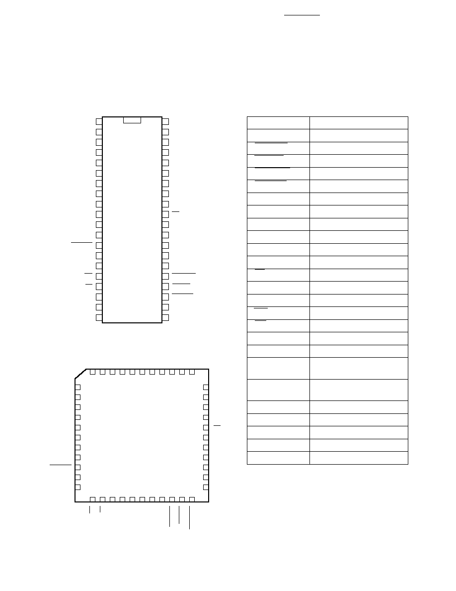
HBCR-1810 Series -- Parallel Pinout
Mnemonic
Description
PP0-PP7
Parallel Port Bits 0-7
CMDRDY
Command Ready
CMDRD
Command Read
DATARDY
Data Ready
DATAWR
Data Write
LED
Control
BPR
Beeper Control
RST
Reset
SI
Scanner Input
SZ
Suppress Zeroes, UPC-E
NC
No Connect
EA
Connect to +5 V
ALE
Address Latch Enable
MDE
Mode
WR
Memory Write
RD
Memory Read
XTAL 1
Crystal Input 1
XTAL 2
Crystal Input 2
C39FLA
Code 39 Full ASCII
Conversion
C39CSE
Code 39 Check Character
Enable
AD0-AD7
Address/Data Bits 0-7
A8
Memory Address Line 8
A9
Memory Address Line 9
V
SS
Ground
V
CC
+5 V Power
PP0
PP1
PP2
PP3
PP4
PP5
PP6
PP7
RST
NC
SZ
SI
CMDRDY
LED
BPR
WR
RD
XTAL 2
XTAL 1
VSS
VCC
AD0
AD1
AD2
AD3
AD4
AD5
AD6
AD7
EA
ALE
NC
MDE - 5 V
C39FLA
C39CSE
DATARDY
CMDRD
DATAWR
A9
A8
1
2
3
4
5
6
7
8
9
10
11
12
13
14
15
16
17
18
19
20
40
39
38
37
36
35
34
33
32
31
30
29
28
27
26
25
24
23
22
21
1810
PP5
1811
6
5
4
3
2
1
44
43
42
41
40
PP6
PP7
RST
NC
NC
SZ
SI
CMDRDY
LED
BPR
39
38
37
36
35
34
33
32
31
30
29
7
8
9
10
11
12
13
14
15
16
17
AD4
AD5
AD6
AD7
EA
NC
ALE
NC
MDE - 5 V
C39FLA
C39CSE
18
19
20 21
22
23
24
25
26
27
28
PP4
PP3
PP2
PP1
PP0
NC
V
CC
AD0
AD1
AD2
AD3
WR
RD
XTAL 2
XTAL 1
V
SS
NC
A8
A9
DATAWR
CMDRD
DATARDY
8
8
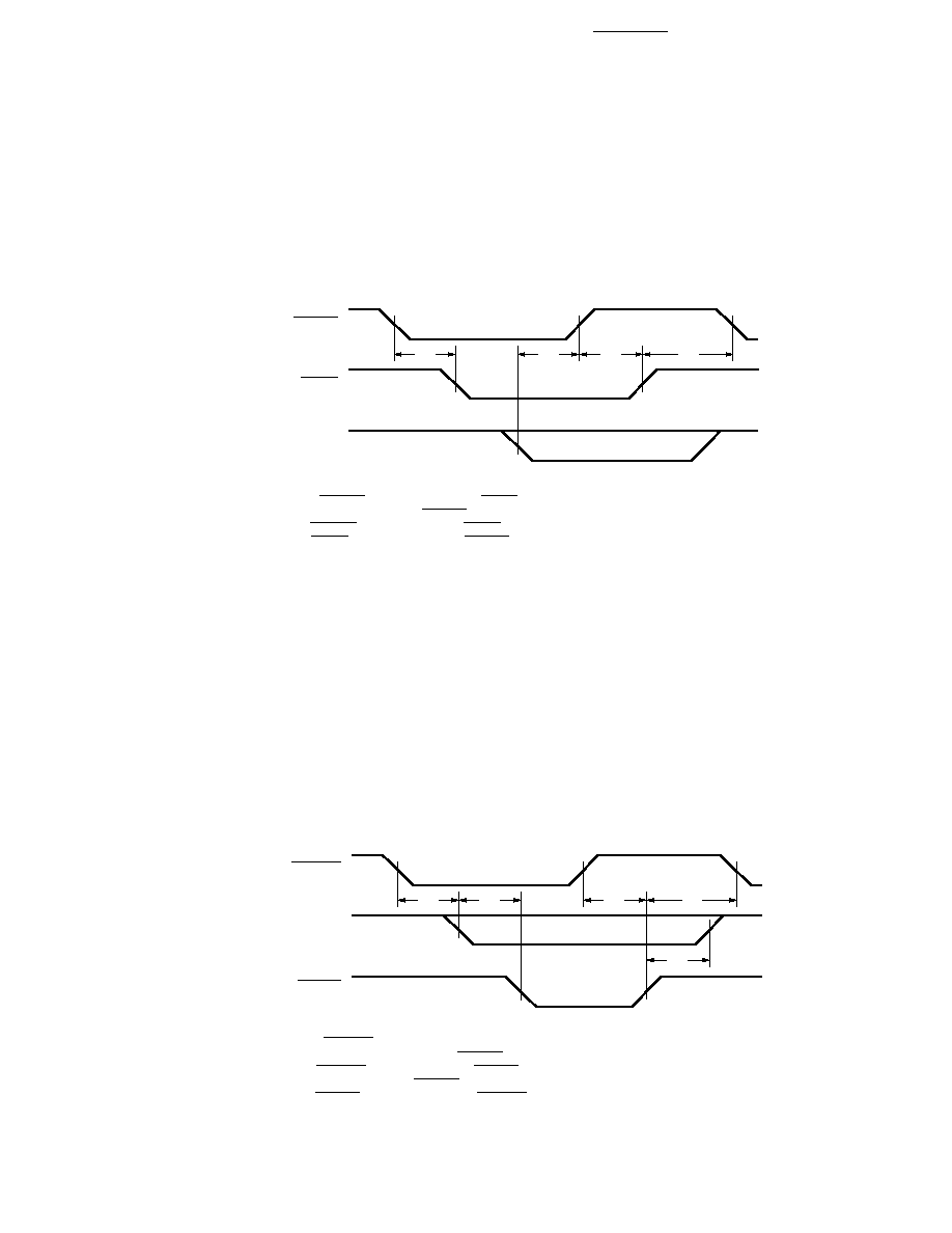
Parallel Mode Handshake Timing
Host Commands Received by Decoder IC
Parallel Mode Handshake Timing
Decoder IC Data Sent to Host
DATARDY
tDO
PORT 1
PINS 0-7
DATAWR
tDF
tDW
tDD
INPUT
FROM HOST
DATA
TO BUS
OUTPUT
TO HOST
DECODER IC DATA SENT TO HOST
tDH
tDO = FALLING EDGE OF DATARDY TO DATA OUTPUT TO BUS. MAXIMUM = 140 µs.
tDF = DATA OUTPUT TO BUS TO FALLING EDGE OF DATAWR. MAXIMUM = 2 µs.
tDW = RISING EDGE OF DATARDY TO RISING EDGE OF DATAWR. MAXIMUM = 5 µs.
tDH = DATA HOLD AFTER RISING EDGE OF DATAWR. MAXIMUM = 2 µs.
tDD = RISING EDGE OF DATAWR TO FALLING EDGE OF DATARDY. MINIMUM = 0 µs.
NOTE:
THESE TIMING SPECIFICATIONS GIVEN ARE BASED ON THE ASSUMPTION THAT THERE IS NO DECODING
IN PROGRESS, NO STATUS, TERMINAL ID, HEADER OR TERMINATOR CHANGE COMMAND IS BEING EXECUTED
AT THE TIME. ALL THE TIMINGS ASSUME THE IC RUNS AT 12 MHz.
CMDRDY
tCR
CMDRD
PORT 1
PINS 0-7
tCA
tCC
INPUT
FROM HOST
OUTPUT
TO HOST
HOST COMMAND
TO BUS
tCR = FALLING EDGE OF CMDRDY TO FALLING EDGE OF CMDRD. MAXIMUM = 22 µs.
tCS = COMMAND SETUP TO RISING EDGE OF CMDRDY. MINIMUM = 0 µs.
tCA = RISING EDGE OF CMDRDY TO RISING EDGE OF CMDRD. TYPICAL = 6 µs.
tCC = RISING EDGE OF CMDRD TO FALLING EDGE OF CMDRDY. MINIMUM = 0 µs.
tCS
NOTE:
THESE TIMING SPECIFICATIONS GIVEN ARE BASED ON THE ASSUMPTION THAT THE SCANNER IS NOT ACTIVE
AT THE TIME. SINCE SCANNER INPUT TO THE IC IS INTERRUPT DRIVEN, THE TIMING MIGHT BE STRETCHED IF
THE SCANNER IS ACTIVE DURING THAT TIME. ALL THE TIMINGS ASSUME THE IC RUNS AT 12 MHz.
9
Escape Sequence Summary
Command
Description
Command
Description
<esc> - y<n>B
Good Read Beep Select
<esc> - y<n>0<text>
Trailer Select
<esc> - y<n>C
Industrial Code Select
<esc> - y<n>S
Status Request
<esc> - y<n>D
Checksum Verification
<esc> - y<n>T
Sound Tone
Select
<esc> - y<n>L
LED Control
<esc> - y<n>U
UPC/EAN/JAN Options
<esc> - y<n>M
Interleaved 2 of 5
<esc> - y<n>W
Scanner Enable
Length Check
<esc> - y<n>N<text>
Header Select
<esc> - y<n>X
DC1/ DC3 Pacing
<esc> E
Hard Reset
Note:
<esc> is the ASCII escape character, 27 decimal, 18 hex.
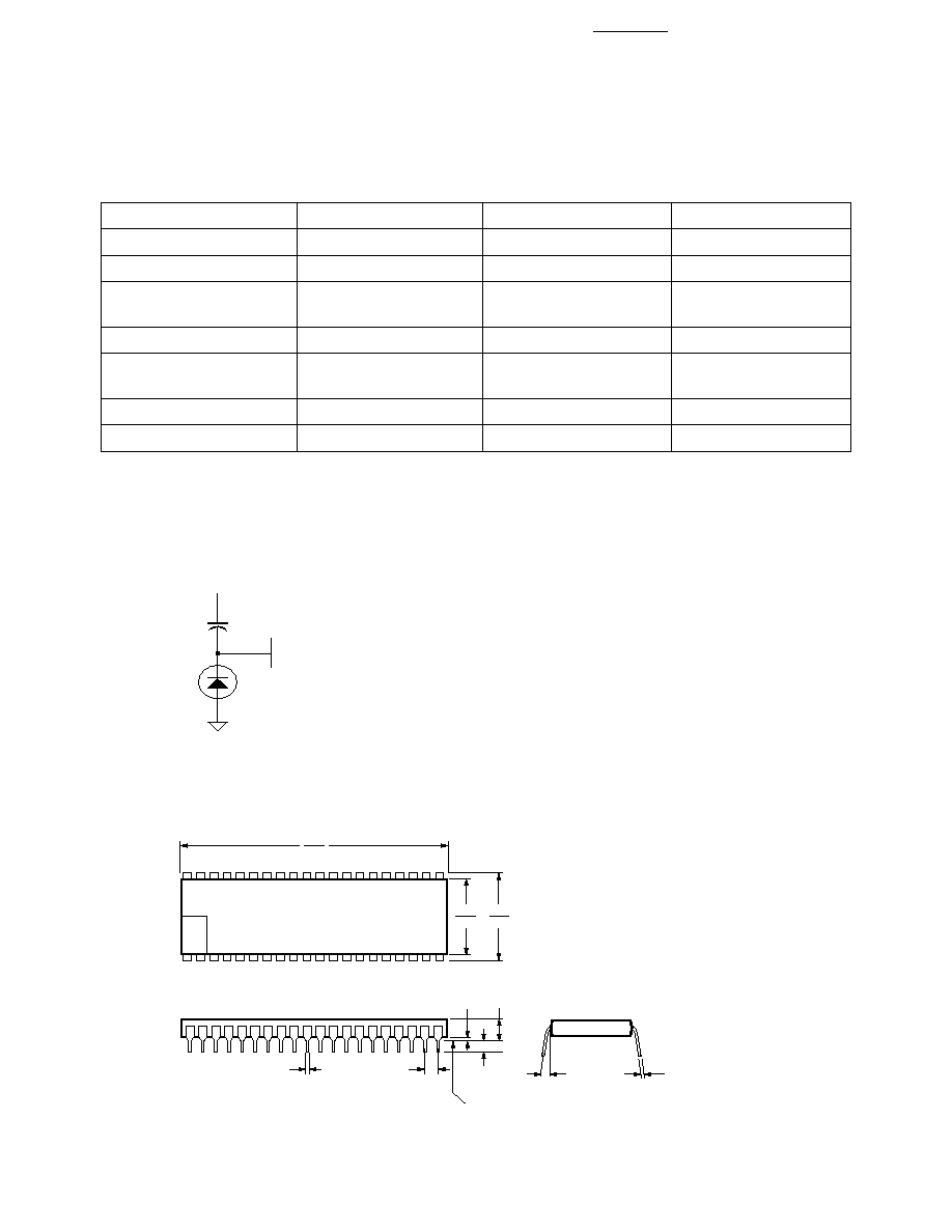
IC Reset Circuits
Figure 1.
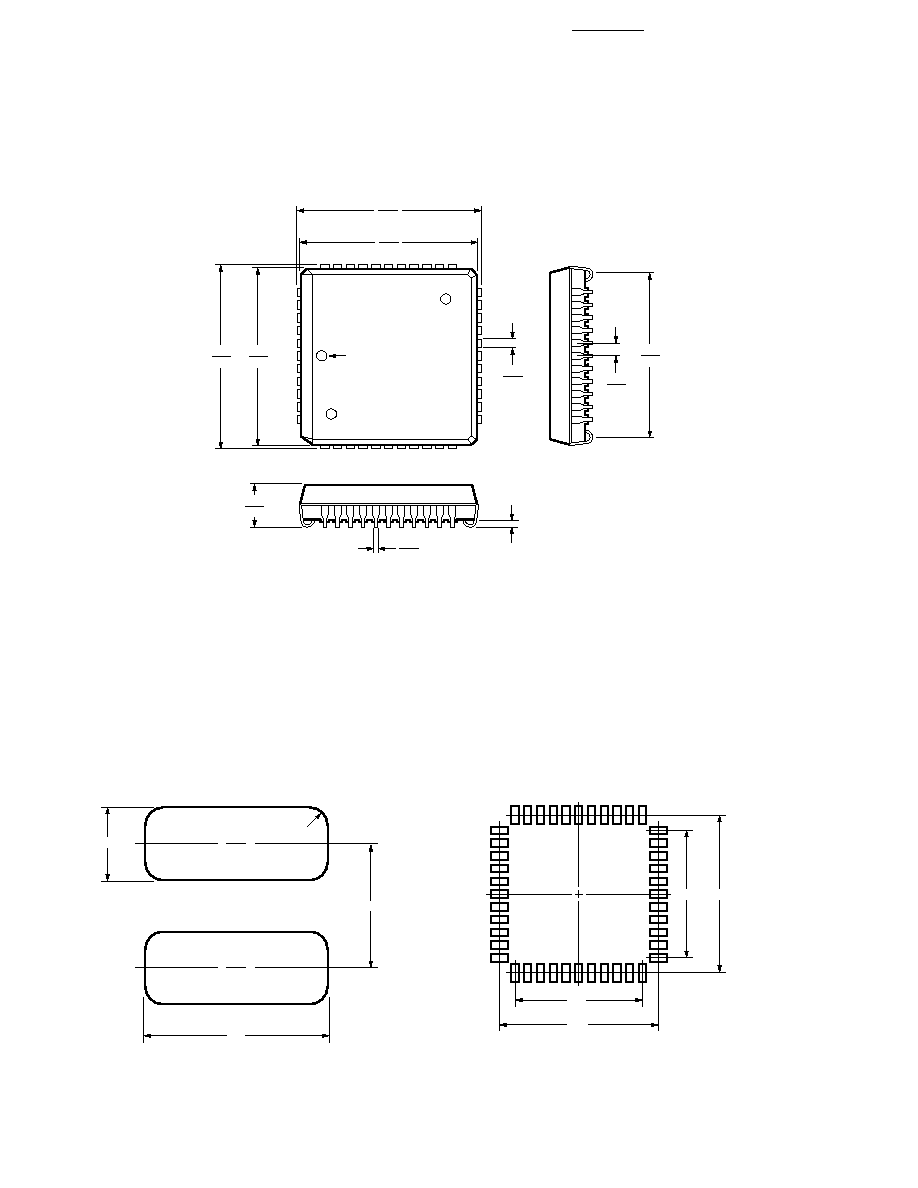
Mechanical Dimensions ≠ Units (mm)
Figure 2. HBCR-1810.
VCC
4.7 µF
1N914
RESET
52.8
51.9
40
21
1
20
14.2
13.6
15.7
14.9
5.1
MAX.
2.54
MAX.
0.3
MIN.
SEATING PLANE
2.54 ± 0.25
0.65 MAX.
0.6 MAX.
UNITS (mm)
0∞ ~ 15∞
INDEX
MARK
AREA
10
10
Figure 3. HBCR-1811.
17.7
17.4
16.0
15.0
UNITS (mm)
16.7
16.5
39
29
17.7
17.4
16.7
16.5
40
6
28
18
7
17
INDEX MARK
1.32
1.22
0.81
0.66
0.53
0.33
4.57
4.20
0.51 MIN.
1
Mechanical Dimensions ≠ Units (mm)
PLCC Solder Pad Reference
Figure 4. Pad Size.
Figure 5. Pad Placement.
0.76
1.8
1.27
R 0.2
UNITS (mm)
12.7
15.6
12.7
15.6
UNITS (mm)
11
PLCC Drying
Whenever Vapor Phase or
Infrared Reflow technologies are
used to mount the PLCC
packages, there is a possibility
that previously absorbed
moisture, heated very rapidly to
the reflow temperatures, may
cause the package to crack from
internal stress. There is a
reliability concern that moisture
may then enter the package over
a period of time, and metal
corrosion may take place,
degrading the IC performance.
To reduce the amount of
absorbed moisture and prevent
cracking, all of the PLCC ICs
should undergo one of the
following baking cycles. The
parts MUST then be mounted
within 48 hours.
If the parts are not mounted
within 48 hours, they MUST be
rebaked.
The total number of baking cycles
must not exceed two (2). If the
ICs are baked more than twice.
Agilent cannot guarantee the
performance and reliability of the
parts.
Cycle
Temperature
Time
Notes
A
125
∞
C
24 Hours
B
60
∞
C
96 Hours
1
Note:
1. Cycle B must be done in an atmosphere of <5 %
relative humidity air or nitrogen.
Neither bake cycle can be
performed in the standard
shipping tubes. The ICs must be
baked in an ESD safe,
mechanically stable container,
such as an aluminum tube or pan.
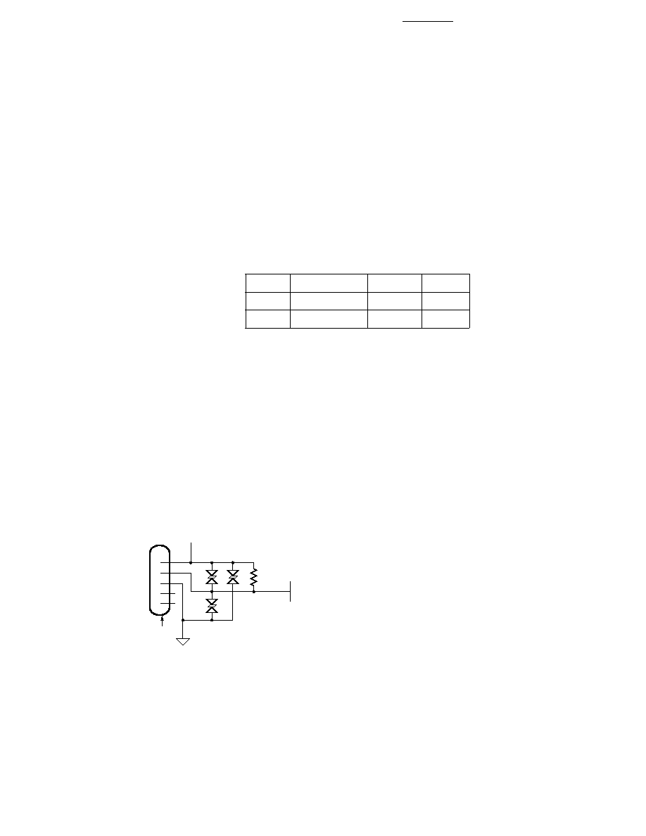
Contact Scanner Input Circuit
VCC
SCANNER
CONNECTOR
SCANNER
INPUT
1
2
3
4
5
SHIELD
1 K
ÆTRANZORBS
P6KE 7.5 C
Figure 6. Recommended Interface.
Notes:
1. The shield MUST be connected to ground for proper scanner operation.
2. The Æ TRANZORBS are optional. If the application requires the frequent changing of the scanners, they are highly recommended.
Æ TRANZORB is a registered trademark of General Semiconductor Industries, Tempe, AZ.
w
Figure 7.
Figure 8.
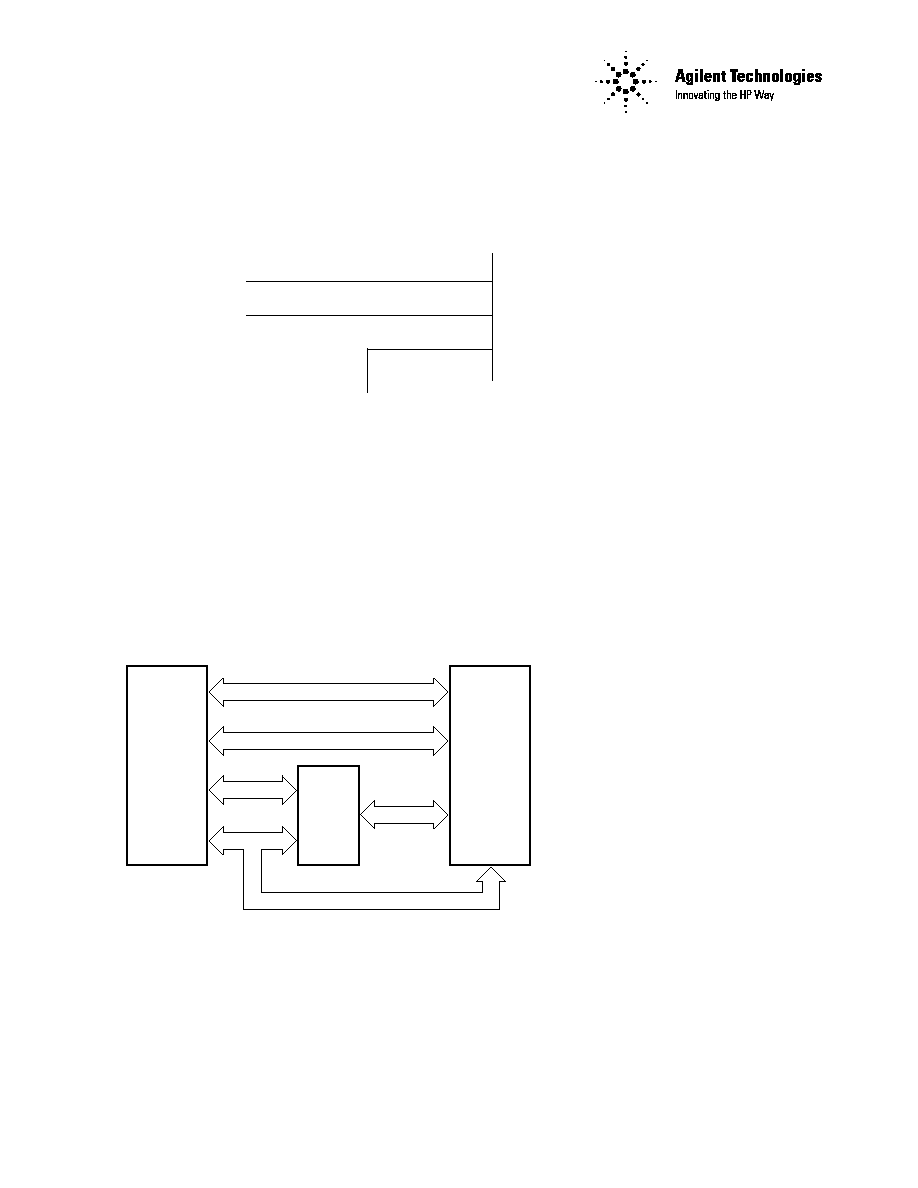
DECODER
IC
DEDICATED
8K x 8
OR
2K x 8
RAM
7
4
3
7
3
ADDRESS/DATA
CONTROL
ADDRESS
ADDRESS
CONTROL
DATA
DEDICATED MEMORY WITH
ADDRESS LATCH CHIP
Block Diagram
External Clock Drivers
No Connect
XTAL2
CMOS Clock
XTAL1
Ground
www.semiconductor.agilent.com
Data subject to change.
Copyright © 1999 Agilent Technologies Inc.
Obsoletes 5954-2182
5968-1076E (11/99)