Dual Channel Line Receiver
Hermetically Sealed
Optocoupler
Technical Data
HCPL-1930
HCPL-1931
HCPL-193K
5962-89572
CAUTION: It is advised that normal static precautions be taken in handling and assembly of this component to
prevent damage and/or degradation which may be induced by ESD.
Description
The HCPL-193X devices are dual
channel, hermetically sealed,
high CMR, line receiver optocoup-
lers. The products are capable of
operation and storage over the
full military temperature range
and can be purchased as either a
standard product or with full
MIL-PRF-38534 Class Level H or
K testing, or from the DSCC
Standard Microcircuit Drawing
(SMD) 5962-89572. This is a
sixteen pin DIP which may be
purchased with a variety of lead
bend and plating options. See
selection guide table for details.
Standard Microcircuit Drawing
(SMD) parts are available for each
lead style.
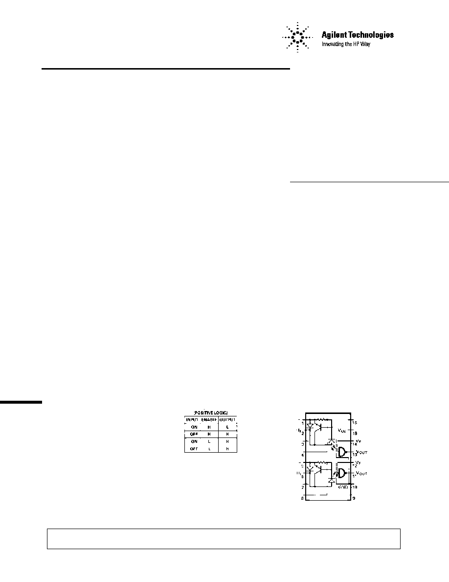
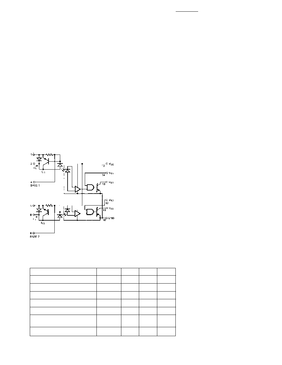
Functional Diagram
Truth Table
Features
∑ Dual Marked with Device
Part Number and DSCC
Standard Microcircuit
Drawing
∑ Manufactured and Tested on
a MIL-PRF-38534 Certified
Line
∑ QML-38534, Class H and
Class K
∑ Hermetically Sealed 16-pin
Dual In-Line Package
∑ Performance Guaranteed
Over -55
∞
C to +125
∞
C
∑ High Speed ≠ 10 Mb/s
∑ Accepts a Broad Range of
Drive Conditions
∑ Adaptive Line Termination
Included
∑ Internal Shield Provides
Excellent Common Mode
Rejection
∑ External Base Lead Allows
"LED Peaking" and LED
Current Adjustment
∑ 1500 Vdc Withstand Test
Voltage
∑ High Radiation Immunity
∑ HCPL-2602 Function
Compatibility
∑ Reliability Data Available
Applications
∑ Military and Space
∑ High Reliability Systems
∑ Isolated Line Receiver
∑ Simplex/Multiplex Data
Transmission
∑ Computer-Peripheral
Interface
∑ Microprocessor System
Interface
∑ Harsh Environmental
Environments
∑ Digital Isolation for A/D,
D/A Conversion
∑ Current Sensing
∑ Instrument Input/Output
Isolation
∑ Ground Loop Elimination
∑ Pulse Transformer
Replacement
The connection of a 0.1
µ
F bypass capacitor between pins 15 and 10 is recommended.
2
DC specifications are compatible
with TTL logic and are guaranteed
from -55
∞
C to +125
∞
C allowing
trouble-free interfacing with
digital logic circuits. An input
current of 10 mA will sink a six
gate fan-out (TTL) at the output
with a typical propagation delay
from input to output of only
45 nsec.
All devices are manufactured and
tested on a MIL-PRF-38534
certified line and are included in
the DSCC Qualified Manufac-
turers List QML-38534 for Hybrid
Microcircuits.
Each unit contains two indepen-
dent channels, consisting of a
GaAsP light emitting diode, an
input current regulator, and an
integrated high gain photon
detector. The input regulator
serves as a line termination for
line receiver applications. It
clamps the line voltage and
regulates the LED current so line
reflections do not interfere with
circuit performance. The regulator
allows a typical LED current of
12.5 mA before it starts to shunt
excess current. The output of the
detector IC is an open collector
Schottky clamped transistor. An
enable input gates the detector.
The internal detector shield
provides a guaranteed common
mode transient immunity specifi-
cation of +1000 V/
µ
sec.
Selection Guide≠Package Styles and Lead
Configuration Options
Agilent Part # and Options
Commercial
HCPL-1930
MIL-PRF-38534 Class H
HCPL-1931
MIL-PRF-38534 Class K
HCPL-193K
Standard Lead Finish
Gold
Solder Dipped
Option #200
Butt Joint/Gold Plate
Option #100
Gull Wing/Soldered
Option #300
Crew Cut/Gold Plate
Option #600
Class H SMD Part #
Prescript for all below
5962-
Either Gold or Soldered
8957201EX
Gold Plate
8957201EC
Solder Dipped
8957201EA
Butt Joint/Gold Plate
8957201YC
Butt Joint/Soldered
8957201YA
Gull Wing/Soldered
8957201XA
Crew Cut/Gold Plate
Available
Crew Cut/Soldered
Available
Class K SMD Part #
Prescript for all below
5962-
Either Gold or Soldered
8957202KEX
Gold Plate
8957202KEC
Solder Dipped
8957202KEA
Butt Joint/Gold Plate
8957202KYC
Butt Joint/Soldered
8957202KYA
Gull Wing/Soldered
8957202KXA
3
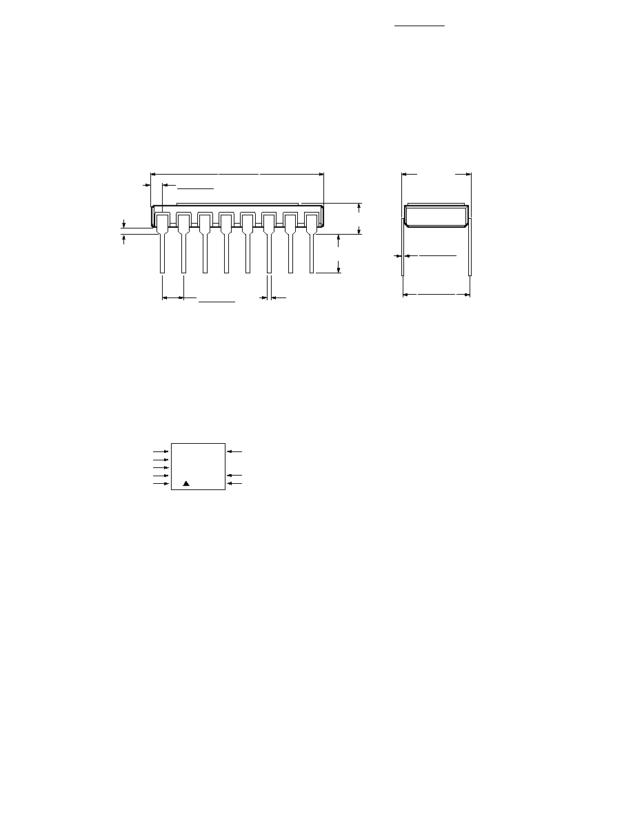
Outline Drawings
16 Pin DIP Through Hole, 2 Channels
Device Marking
4.45 (0.175)
MAX.
20.06 (0.790)
20.83 (0.820)
0.51 (0.020)
MAX.
2.29 (0.090)
2.79 (0.110)
0.51 (0.020)
MIN.
0.89 (0.035)
1.65 (0.065)
8.13 (0.320)
MAX.
7.36 (0.290)
7.87 (0.310)
0.20 (0.008)
0.33 (0.013)
NOTE: DIMENSIONS IN MILLIMETERS (INCHES).
3.81 (0.150)
MIN.
COMPLIANCE INDICATOR,*
DATE CODE, SUFFIX (IF NEEDED)
A QYYWWZ
XXXXXX
XXXXXXX
XXX XXX
50434
COUNTRY OF MFR.
Agilent CAGE CODE*
Agilent DESIGNATOR
DSCC SMD*
PIN ONE/
ESD IDENT
Agilent P/N
DSCC SMD*
* QUALIFIED PARTS ONLY
4
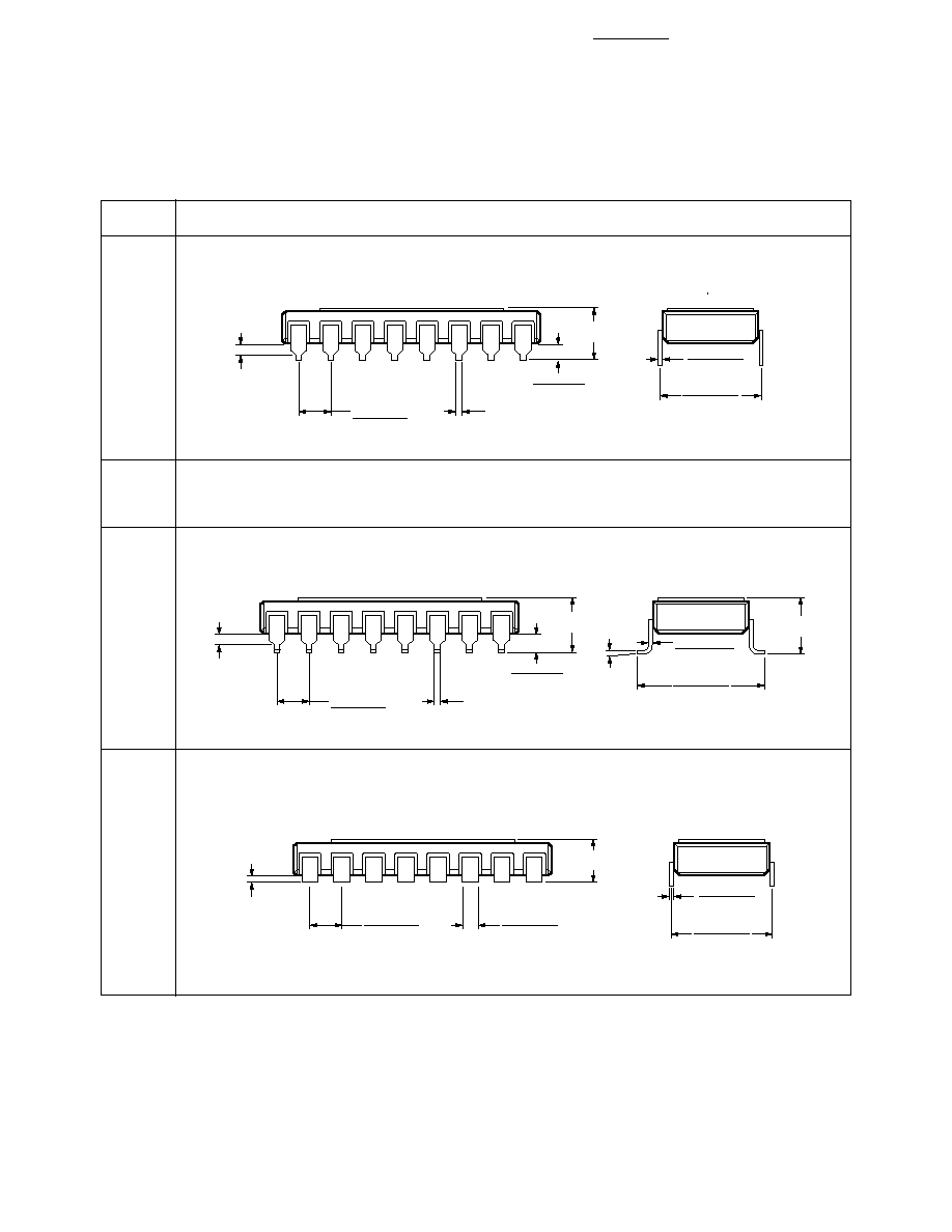
Option
Description
Hermetic Optocoupler Options
100
Surface mountable hermetic optocoupler with leads trimmed for butt joint assembly. This option
is available on commercial and hi-rel product.
200
Lead finish is solder dipped rather than gold plated. This option is available on commercial and
hi-rel product. DSCC Drawing part numbers contain provisions for lead finish.
300
Surface mountable hermetic optocoupler with leads cut and bent for gull wing assembly. This
option is available on commercial and hi-rel product. This option has solder dipped leads.
600
Surface mountable hermetic optocoupler with leads trimmed for butt joint assembly. This option
is available on commercial and hi-rel product. Contact factory for the availability of this option
on DSCC part types.
Note: Dimensions in millimeters (inches).
3.81 (0.150)
MIN.
1.14 (0.045)
1.25 (0.049)
2.29 (0.090)
2.79 (0.110)
0.51 (0.020)
MIN.
7.36 (0.290)
7.87 (0.310)
0.20 (0.008)
0.33 (0.013)
1.14 (0.045)
1.40 (0.055)
4.32 (0.170)
MAX.
0.51 (0.020)
MAX.
2.29 (0.090)
2.79 (0.110)
0.51 (0.020)
MIN.
7.36 (0.290)
7.87 (0.310)
0.20 (0.008)
0.33 (0.013)
1.40 (0.055)
1.65 (0.065)
4.57 (0.180)
MAX.
0.51 (0.020)
MAX.
2.29 (0.090)
2.79 (0.110)
0.51 (0.020)
MIN.
9.65 (0.380)
9.91 (0.390)
0.20 (0.008)
0.33 (0.013)
5∞ MAX.
4.57 (0.180)
MAX.
5
Absolute Maximum Ratings
Storage Temperature ................................................. -65
∞
C to +150
∞
C
Operating Temperature ............................................... -55
∞
C to +125
∞
C
Lead Solder Temperature ................................................ 260
∞
C for 10 s
1.6 mm below seating plane
Forward Input Current ≠ I
I
(each channel) ................................. 60 mA
2
Reverse Input Current ................................................................. 60 mA
Supply Voltage ≠ V
CC
....................................... 7 V (1 Minute Maximum)
Enable Input Voltage ≠ V
E
(each channel) ...................................... 5.5 V
Not to exceed V
CC
by more than 500 mV
Output Collector Current ≠ I
O
(each channel) ............................. 25 mA
Output Collector Power Dissipation (each channel) ................... 40 mW
Output Collector Voltage ≠ V
O
(each channel) ................................... 7 V
Total Package Power Dissipation .............................................. 564 mW
Input Power Dissipation (each channel) ................................... 168 mW
Parameter
Symbol
Min.
Max.
Units
Input Current, Low Level
I
IL
0
250
µ
A
Input Current, High Level*
I
IH
12.5
60
mA
Supply Voltage, Output
V
CC
4.5
5.5
V
High Level Enable Voltage
V
EH
2.0
V
CC
V
Low Level Enable Voltage
V
EL
0
0.8
V
Fan Out (@ R
L
= 4 k
)
N
5
TTL
Loads
Operating Temperature
T
A
-55
125
∞
C
*12.5 mA condition permits at least 20% guardband for optical coupling variation. Initial
switching threshold is 10 mA or less.
Recommended Operating Conditions
ESD Classification
(MIL-STD-883, Method 3015) .............................................. (
), Class 1
Schematic
A 0.1
µ
F BYPASS CAPACITOR
MUST BE CONNECTED BETWEEN
PINS 10 AND 15 (SEE NOTE 1).