
Description
These diode-transistor optocouplers
use an insulating layer between a
LED and an integrated
photodetector to provide electrical
insulation between input and
output. Separate connections for
the photodiode bias and output-
transistor collector increase the
speed up to a hundred times that of
a conventional phototransistor
coupler by reducing the base-
collector capacitance.
Agilent HCPL-250L/ 050L/253L/053L
LVTTL/LVCMOS Compatible 3.3 V
Optocouplers (1 Mb/s)
Data Sheet
Features
∑ Low power consumption
∑ High speed: 1 Mb/s
∑ LVTTL/LVCMOS compatible
∑ Available in 8-pin DIP, SO-8
∑ Open collector output
∑ Guaranteed performance from
temperature: 0∞C to +70∞C
∑ Safety approval, UL, CSA, IEC/EN/DIN
EN 60747-5-2
Applications
∑ High voltage insulation
∑ Video signal isolation
∑ Power translator isolation in motor
drives
∑ Line receivers
∑ Feedback element in switched mode
power supplies
∑ High speed logic ground isolation ≠
LVTTL/LVCMOS
∑ Replaces pulse transformers
∑ Replaces slow phototransistor
isolators
∑ Analog signal ground isolation
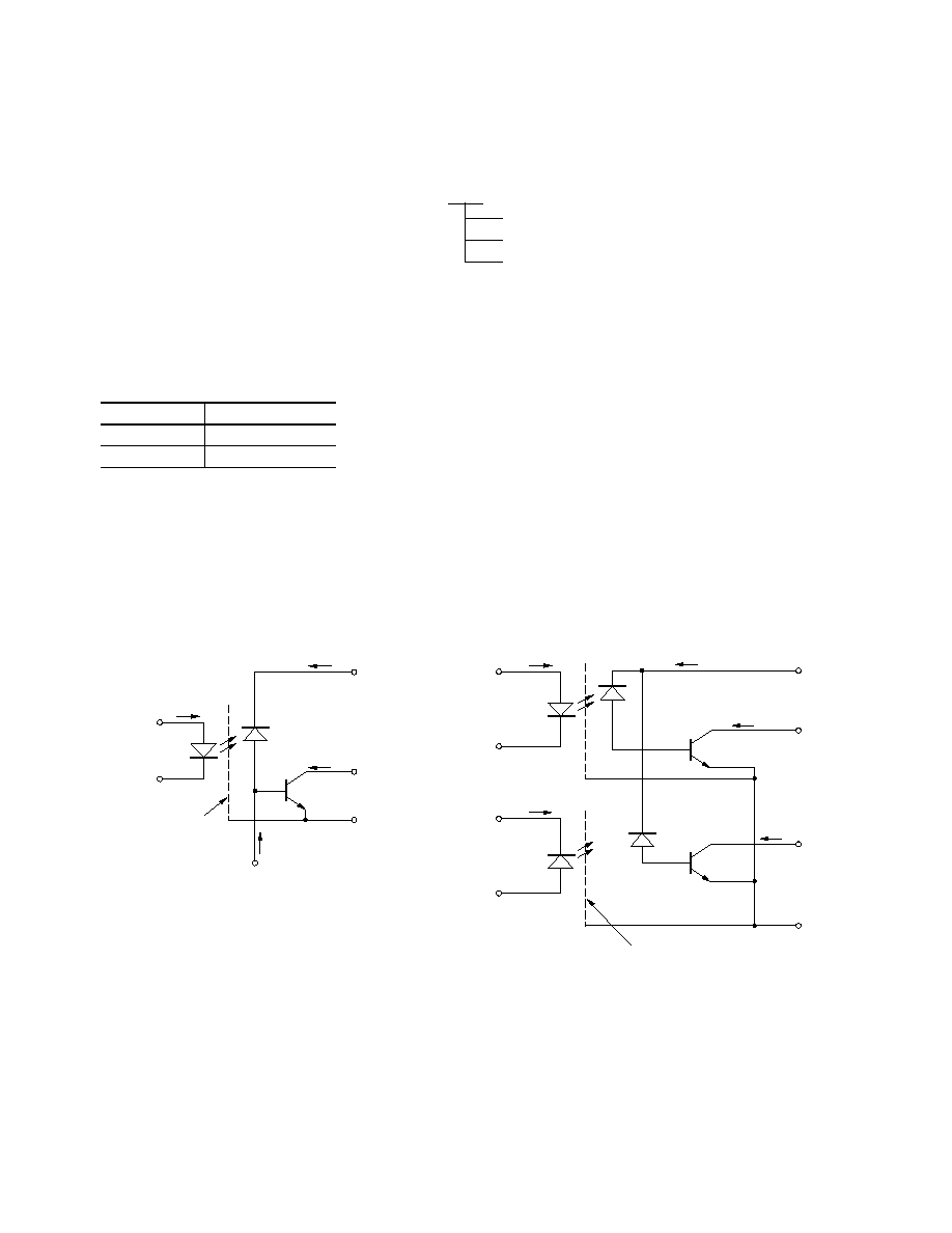
Functional Diagram
A 0.1
µ
F bypass capacitor must be connected between pins 5 and 8.
CAUTION: It is advised that normal static precautions be taken in handling and assembly of this component to prevent
damage and/or degradation which may be induced by ESD.
These optocouplers are available
in an 8-pin DIP and in an industry
standard SO-8 package. The
following is a cross reference
table listing the 8-pin DIP part
number and the electrically
equivalent SO-8 part number.
The SO-8 does not require
"through holes" in a PCB. This
package occupies approximately
one-third the footprint area of the
7
1
2
3
4
5
6
8
ANODE 1
CATHODE 1
CATHODE 2
ANODE 2
VCC
VO1
VO2
GND
HCPL≠253L/HCPL≠053L
7
1
2
3
4
5
6
8
NC
ANODE
CATHODE
NC
VCC
VB
VO
GND
TRUTH TABLE
(POSITIVE LOGIC)
LED
ON
OFF
VO
LOW
HIGH
HCPL≠250L/HCPL≠050L
2
Ordering Information
Specify Part Number followed by Option Number (if desired).
Example:
HCPL-250L #XXXX
060 = IEC/EN/DIN EN 60747-5-2 V
IORM
500 = Tape and Reel Packaging Option
XXXE = Lead Free Option
Option data sheets available. Contact Agilent sales representative or
authorized distributor for information.
Schematic
standard dual-in-line package.
The lead profile is designed to be
compatible with standard surface
mount processes.
These optocouplers can be used
in LVTTL/LVCMOS or wide
bandwidth analog applications.
The common mode transient
immunity of 1000 V/
µ
s minimum
to typical at V
CM
= 10 V
guaranteed for these
optocouplers.
8-Pin DIP
SO-8 Package
HCPL-250L
HCPL-050L
HCPL-253L
HCPL-053L
IF1
SHIELD
8
7
VCC
+
2
VO1
ICC
VF1
I O1
1
≠
IF2
6
5
GND
≠
4
VO2
VF2
I O2
3
+
IF
SHIELD
8
6
5
GND
VCC
2
3
VO
ICC
VF
IO
ANODE
CATHODE
+
≠
7
VB
IB
*
HCPL-250L/HCPL-050L
HCPL-253L/HCPL-053L
Remarks: The notation "#" is used for existing products, while (new)
products launched since 15th July 2001 and lead free option will use "-"
3
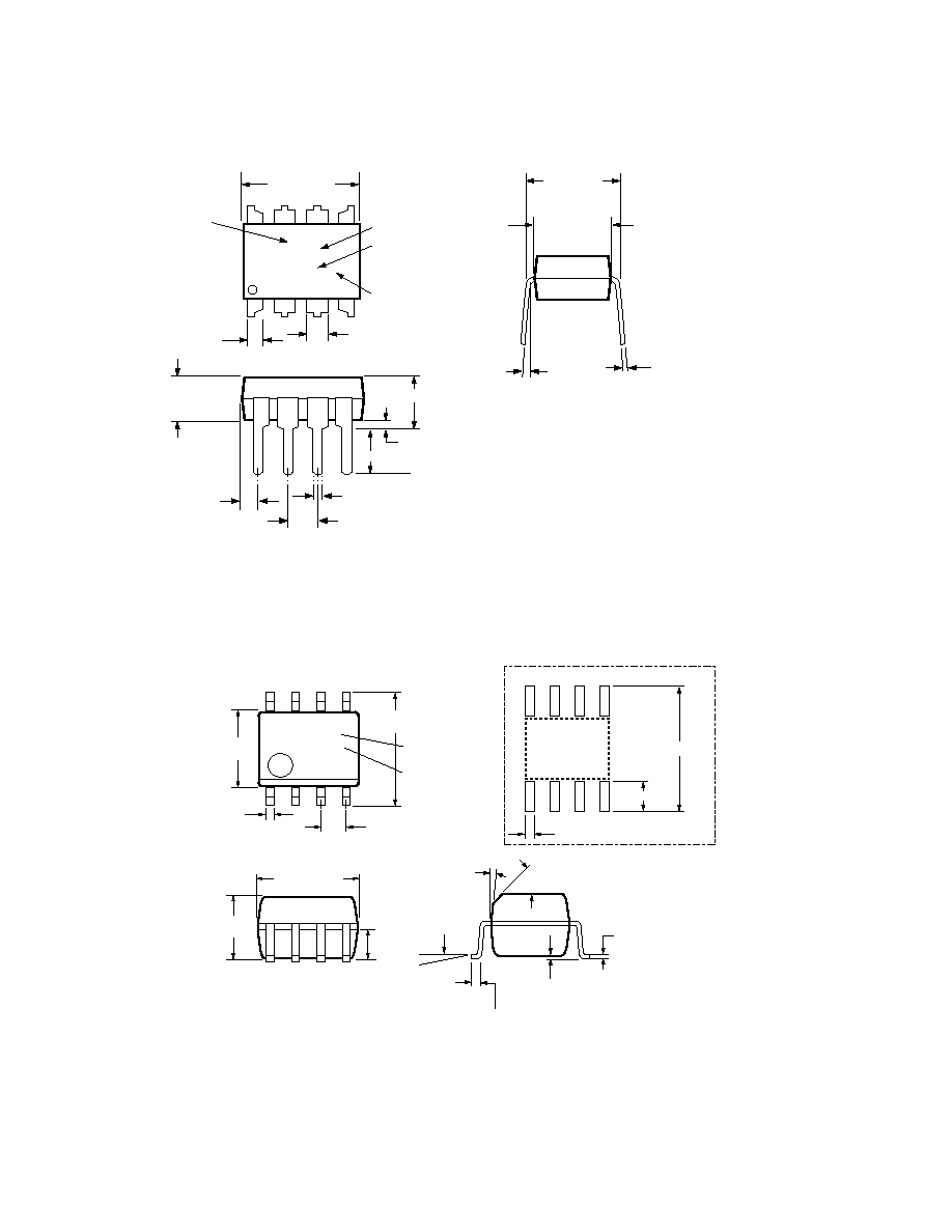
Package Outline Drawings
8-Pin DIP Package
1.080 ± 0.320
(0.043 ± 0.013)
2.54 ± 0.25
(0.100 ± 0.010)
0.51 (0.020) MIN.
0.65 (0.025) MAX.
4.70 (0.185) MAX.
2.92 (0.115) MIN.
5∞ TYP.
0.254
+ 0.076
- 0.051
(0.010
+ 0.003)
- 0.002)
7.62 ± 0.25
(0.300 ± 0.010)
6.35 ± 0.25
(0.250 ± 0.010)
9.65 ± 0.25
(0.380 ± 0.010)
1.78 (0.070) MAX.
1.19 (0.047) MAX.
A XXXXZ
YYWW
DATE CODE
DIMENSIONS IN MILLIMETERS AND (INCHES).
5
6
7
8
4
3
2
1
OPTION CODE*
UL
RECOGNITION
UR
TYPE NUMBER
* MARKING CODE LETTER FOR OPTION NUMBERS
"V" = OPTION 060
OPTION NUMBERS 300 AND 500 NOT MARKED.
NOTE: FLOATING LEAD PROTRUSION IS 0.25 mm (10 mils) MAX.
3.56 ± 0.13
(0.140 ± 0.005)
Small Outline SO-8 Package
XXXV
YWW
8
7
6
5
4
3
2
1
5.994 ± 0.203
(0.236 ± 0.008)
3.937 ± 0.127
(0.155 ± 0.005)
0.406 ± 0.076
(0.016 ± 0.003)
1.270
(0.050)
BSC
5.080 ± 0.127
(0.200 ± 0.005)
3.175 ± 0.127
(0.125 ± 0.005)
1.524
(0.060)
45∞ X
0.432
(0.017)
0.228 ± 0.025
(0.009 ± 0.001)
TYPE NUMBER
(LAST 3 DIGITS)
DATE CODE
0.305
(0.012)
MIN.
TOTAL PACKAGE LENGTH (INCLUSIVE OF MOLD FLASH)
5.207 ± 0.254 (0.205 ± 0.010)
DIMENSIONS IN MILLIMETERS (INCHES).
LEAD COPLANARITY = 0.10 mm (0.004 INCHES) MAX.
OPTION NUMBER 500 NOT MARKED.
NOTE: FLOATING LEAD PROTRUSION IS 0.15 mm (6 mils) MAX.
0.203 ± 0.102
(0.008 ± 0.004)
7∞
PIN ONE
0 ~ 7∞
*
*
7.49 (0.295)
1.9 (0.075)
0.64 (0.025)
LAND PATTERN RECOMMENDATION
4
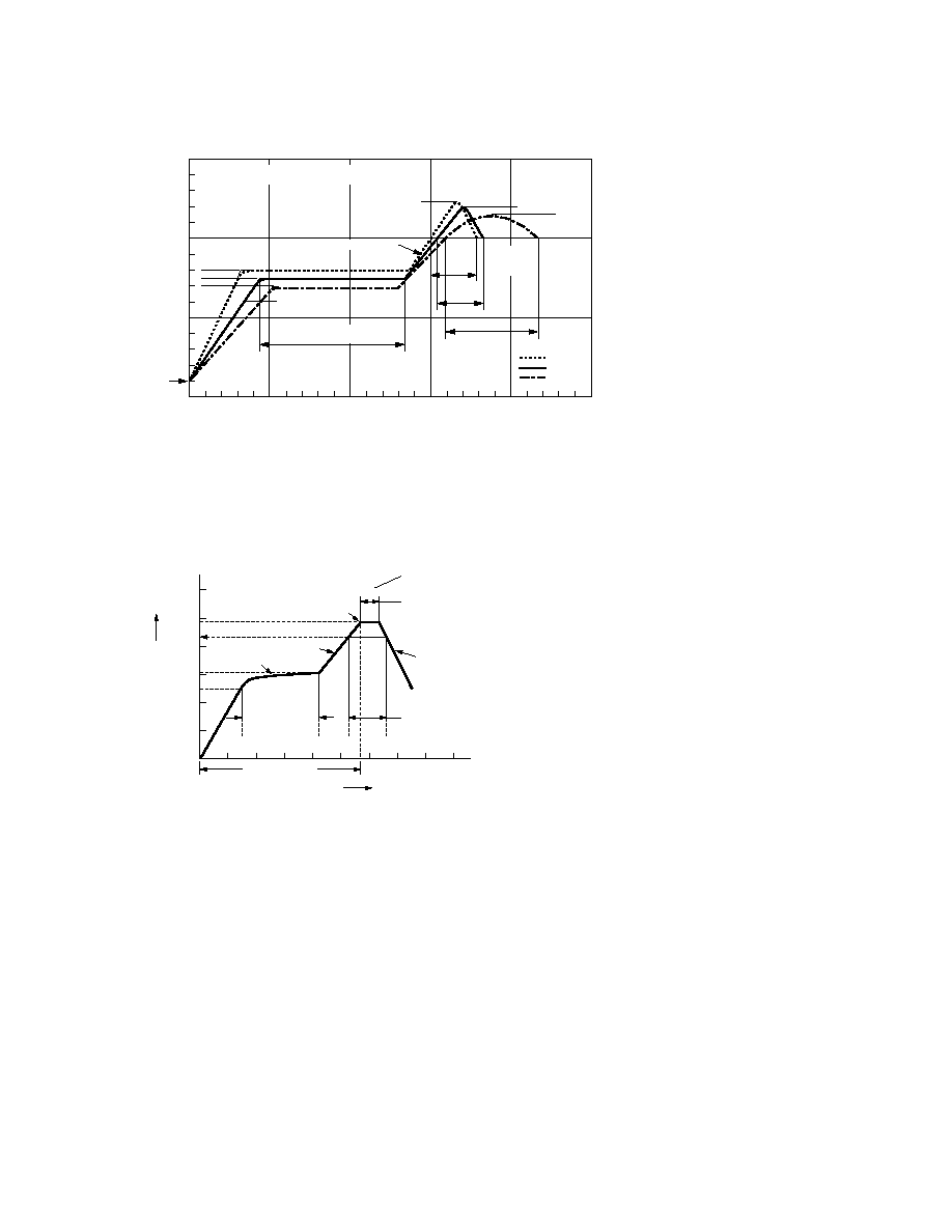
Solder Reflow Temperature Profile
Regulatory Information
The devices contained in this
data sheet have been approved by
the following organizations:
UL
Approval under UL 1577,
Component Recognition
Program, File E55361.
CSA
Approval under CSA Component
Acceptance
Notice #5, File CA 88324.
IEC/EN/DIN EN 60747-5-2
Approved under :
IEC 60747-5-2:1997 + A1:2002
EN 60747-5-2:2001 + A1:2002
DIN EN 60747-5-2 (VDE 0884
Teil 2):2003-01
Recommended Pb-Free IR Profile
0
TIME (SECONDS)
TEMPERATURE (
∞
C)
200
100
50
150
100
200
250
300
0
30
SEC.
50 SEC.
30
SEC.
160∞C
140∞C
150∞C
PEAK
TEMP.
245∞C
PEAK
TEMP.
240∞C
PEAK
TEMP.
230∞C
SOLDERING
TIME
200∞C
PREHEATING TIME
150∞C, 90 + 30 SEC.
2.5∞C ± 0.5∞C/SEC.
3∞C + 1∞C/≠0.5∞C
TIGHT
TYPICAL
LOOSE
ROOM
TEMPERATURE
PREHEATING RATE 3∞C + 1∞C/≠0.5∞C/SEC.
REFLOW HEATING RATE 2.5∞C ± 0.5∞C/SEC.
217 ∞C
RAMP-DOWN
6 ∞C/SEC. MAX.
RAMP-UP
3 ∞C/SEC. MAX.
150 - 200 ∞C
260 +0/-5 ∞C
t 25 ∞C to PEAK
60 to 150 SEC.
20-40 SEC.
TIME WITHIN 5 ∞C of ACTUAL
PEAK TEMPERATURE
tp
ts
PREHEAT
60 to 180 SEC.
tL
TL
Tsmax
Tsmin
25
Tp
TIME
TEMPERA
TURE
NOTES:
THE TIME FROM 25 ∞C to PEAK TEMPERATURE = 8 MINUTES MAX.
Tsmax = 200 ∞C, Tsmin = 150 ∞C

5
Insulation and Safety Related Specifications
8-Pin DIP
(300 Mil)
SO-8
Parameter
Symbol
Value
Value
Units
Conditions
Minimum External Air
L (101)
7.1
4.9
mm
Measured from input terminals to output
Gap (External Clearance)
terminals, shortest distance through air.
Minimum External Tracking
L (102)
7.4
4.8
mm
Measured from input terminals to output
(External Creepage)
terminals, shortest distance path along body.
Minimum Internal Plastic
0.08
0.08
mm
Through insulation distance, conductor to
Gap (Internal Clearance)
conductor, usually the direct distance
between the photoemitter and photodetector
inside the optocoupler cavity.
Tracking Resistance
CTI
200
200
Volts
DIN IEC 112/VDE 0303 Part 1
(Comparative Tracking
Index)
Isolation Group
IIIa
IIIa
Material Group (DIN VDE 0110, 1/89, Table 1)
IEC/EN/DIN EN 60747-5-2Insulation Related Characteristics
Description
Symbol
PDIP Option 060
SO-8 Option 60
Units
Installation classification per DIN VDE 0110/1.89, Table 1
for rated mains voltage
150 V rms
I-IV
for rated mains voltage
300 V rms
I-IV
I-III
for rated mains voltage
600 V rms
I-III
I-II
Climatic Classification
55/85/21
55/85/21
Pollution Degree (DIN VDE 0110/1.89)
2
2
Maximum Working Insulation Voltage
V
IORM
630
566
V
peak
Input to Output Test Voltage, Method b*
V
IORM
x 1.875 = V
PR
, 100% Production Test
V
PR
1181
1063
V
peak
with t
m
= 1 sec, Partial Discharge < 5 pC
Input to Output Test Voltage, Method a*
V
IORM
x 1.5 = V
PR
, Type and Sample Test,
V
PR
945
849
V
peak
t
m
= 60 sec, Partial Discharge < 5 pC
Highest Allowable Overvoltage*
V
IOTM
6000
4000
V
peak
(Transient Overvoltage, t
ini
= 10 sec)
Safety Limiting Values
(Maximum values allowed in the event of a failure,
also see Figure 16, Thermal Derating curve.)
Case Temperature
T
S
175
150
∞C
Input Current
I
S,INPUT
230
150
mA
Output Power
P
S,OUTPUT
600
600
mW
Insulation Resistance at T
S
, V
IO
= 500 V
R
S
10
9
10
9
*Refer to the front of the optocoupler section of the current catalog, under Product Safety Regulations section, IEC/EN/DIN EN 60747-5-2, for a
detailed description.
Note: Isolation characteristics are guaranteed only within the safety maximum ratings which must be ensured by protective circuits in application.

6
Absolute Maximum Ratings
Parameter
Symbol
Min.
Max.
Units
Note
Storage Temperature
T
S
≠55
125
∞
C
Operating Temperature
T
A
≠55
100
∞
C
≠55
85
Average Forward Input Current
I
F(AVG)
25
mA
1
Peak Forward Input Current
I
F(PEAK)
2
(50% duty cycle, 1 ms pulse width)
50
mA
(50% duty cycle, 1 ms pulse width)
40
Peak Transient Input Current
I
F(TRANS)
1
A
(
1
µ
s pulse width, 300 pps)
0.1
Reverse LED Input Voltage (Pin 3-2)
V
R
5
V
Input Power Dissipation
P
IN
45
mW
3
4
Average Output Current (Pin 6)
I
O(AVG)
8
mA
Peak Output Current
I
O(PEAK)
16
mA
Emitter-Base Reverse Voltage
V
EBR
5
V
Supply Voltage (Pin 8-5)
V
CC
≠0.5
7
V
Output Voltage (Pin 6-5)
V
O
≠0.5
7
V
Base Current
I
B
5
mA
Output Power Dissipation
P
O
100
mW
4
Lead Solder Temperature
(Through Hole Parts Only)
1.6 mm below seating plane, 10 sec.
T
LS
260
∞
C
up to seating plane, 10 seconds
260
∞
C
Reflow Temperature Profile
T
RP
See Package Outline Drawings
section
Recommended Operating Conditions
Parameter
Symbol
Min.
Max.
Units
Power Supply Voltage
V
CC
2.7
3.6
V
Forward Input Current
I
F(ON)
16
20
mA
Forward Input Voltage
V
F(OFF)
0
0.8
V
Operating Temperature
T
A
0
85
∞
C

7
Electrical Specifications (DC)
Over Recommended Temperature (T
A
= 0∞C to +70∞C), V
CC
= 3.3 V, I
F
= 16 mA, unless otherwise specified. See Note 13.
Parameter
Sym. Device Min. Typ.
Max.
Units
Test Conditions
Fig.
Note
Current Transfer CTR
%
T
A
= 25∞C
V
O
= 0.4 V
I
F
= 16 mA,
2
5, 11
V
CC
= 3.3 V
15
20
50
Logic Low
V
OL
V
I
F
= 16 mA,
V
CC
= 3.3 V
0.05
0.3
T
A
= 25∞C
I
O
= 3.0 mA
Logic High
I
OH
0.003 1
µ
A
T
A
= 25∞C
V
O
= V
CC
= 3.3 V I
F
= 0 mA
3
Output Current
Logic Low
I
CCL
43.0
100
µ
A
I
F
= 16 mA, V
O
= Open, V
CC
= 3.3 V
13
Supply Current
Dual
300
Logic High
I
CCH
0.005 0.3
µ
A
T
A
= 25∞C
I
F
= 0 mA, V
O
= Open,
13
Supply Current
Dual
10
V
CC
= 3.3 V
Input Forward
V
F
1.52
1.7
V
T
A
= 25∞C
I
F
= 16 mA
1
Voltage
Input Reverse
BV
R
5
V
I
R
= 10
µ
A
Breakdown
Voltage
Input
C
IN
60
pF
f = 1 MHz, V
F
= 0 V
Capacitance
Ratio
Output Voltage
Switching Specifications (AC)
Over Recommended Temperature (T
A
= 0∞C to +70∞C), V
CC
= 3.3 V, I
F
= 16 mA unless otherwise specified.
All typicals at V
CC
= 3.3 V, T
A
= 25
∞
C.
Parameter
Sym.
Device Min. Typ.*
Max.
Units
Test Conditions
Fig.
Note
Propagation
t
PHL
0.35
1
µ
s
R
L
= 1.9 k
5
8, 9
Delay Time to
Logic Low at
Output
Propagation
t
PLH
0.65
1
µ
s
R
L
= 1.9 k
5
8, 9
Delay Time to
Logic High at
Output
Common Mode |CM
H
|
1
kV/
µ
s
R
L
= 4.1 k
I
F
= 0 mA, T
A
= 25∞C,
6
7, 8, 9
Transient
R
L
= 1.9 k
V
CM
= 10 V
p-p
Immunity at
C
L
= 15 pF
Logic High
Level Output
Common Mode |CM
L
|
1
kV/
µ
s
R
L
= 4.1 k
I
F
= 16 mA, T
A
= 25∞C,
6
7, 8, 9
Transient
R
L
= 1.9 k
V
CM
= 10 V
p-p
Immunity at
C
L
= 15 pF
Logic Low
Level Output
*All typicals at T
A
= 25∞C

8
Package Characteristics
Over Recommended Temperature (T
A
= 0∞C to 70∞C) unless otherwise specified.
Parameter
Sym.
Device
Min.
Typ.* Max.
Units
Test Conditions
Fig.
Note
Input-Output
V
ISO
8-Pin DIP
3750
V rms
RH < 50%,
6, 14
Momentary
SO-8
t = 1 min.,
Withstand
T
A
= 25∞C
Voltage**
I
I-O
8-Pin DIP
1
µ
A
45% RH, t = 5 s,
6, 16
V
I-O
= 3 kVdc,
T
A
= 25∞C
Input-Output
R
I-O
8-Pin DIP
10
12
V
I-O
= 500 Vdc
6
Resistance
SO-8
Input-Output
C
I-O
8-Pin DIP
0.6
pF
f = 1 MHz
6
Capacitance
SO-8
*All typicals at T
A
= 25∞C.
**The Input-Output Momentary Withstand Voltage is a dielectric voltage rating that should not be interpreted as an input-output continuous
voltage rating. For the continuous voltage rating refer to the IEC/EN/DIN EN 60747-5-2 Insulation Related Characteristics Table (if applicable),
your equipment level safety specification or Agilent Application Note 1074 entitled "Optocoupler Input-Output Endurance Voltage," publication
number 5963-2203E.
Notes:
1. Derate linearly above 70∞C free-air temperature at a rate of 0.8 mA/∞C (8-Pin DIP).
Derate linearly above 85∞C free-air temperature at a rate of 0.5 mA/∞C (SO-8).
2. Derate linearly above 70∞C free-air temperature at a rate of 1.6 mA/∞C (8-Pin DIP).
Derate linearly above 85∞C free-air temperature at a rate of 1.0 mA/∞C (SO-8).
3. Derate linearly above 70∞C free-air temperature at a rate of 0.9 mW/∞C (8-Pin DIP).
Derate linearly above 85∞C free-air temperature at a rate of 1.1 mW/∞C (SO-8).
4. Derate linearly above 70∞C free-air temperature at a rate of 2.0 mW/∞C (8-Pin DIP).
Derate linearly above 85∞C free-air temperature at a rate of 2.3 mW/∞C (SO-8).
5. CURRENT TRANSFER RATIO in percent is defined as the ratio of output collector current, I
O
, to the forward LED input current, I
F
, times 100.
6. Device considered a two-terminal device: Pins 1, 2, 3, and 4 shorted together and Pins 5, 6, 7, and 8 shorted together.
7. Common mode transient immunity in a Logic High level is the maximum tolerable (positive) dV
CM
/dt on the leading edge of the common
mode pulse signal, V
CM
, to assure that the output will remain in a Logic High state (i.e., V
O
> 2.0 V). Common mode transient immunity in a
Logic Low level is the maximum tolerable (negative) dV
CM
/dt on the trailing edge of the common mode pulse signal, V
CM
, to assure that the
output will remain in a Logic Low state (i.e., V
O
< 0.8 V).
8. The 1.9 k
load represents 1 TTL unit load of 1.6 mA and the 5.6 mA k
pull-up resistor.
9. The 4.1 k
load represents 1 LSTTL unit load of 0.36 mA and 6.1 k
pull-up resistor.
10. The frequency at which the AC output voltage is 3 dB below its mid-frequency value.
11. The JEDEC registration for the 6N136 specifies a minimum CTR of 15%. Agilent guarantees a minimum CTR of 15%.
12. See Option 020 data sheet for more information.
13. Use of a 0.1
µ
f bypass capacitor connected between pins 5 and 8 is recommended.
14. In accordance with UL 1577, each optocoupler is proof tested by applying an insulation test voltage
4500 V rms for 1 second (leakage
detection current limit, I
I-O
5
µ
A). This test is performed before the 100% Production test shown in the IEC/EN/DIN EN 60747-5-2 Insulation
Related Characteristics Table, if applicable.
15. In accordance with UL 1577, each optocoupler is proof tested by applying an insulation test voltage
6000 V rms for 1 second (leakage
detection current limit, I
I-O
5
µ
A). This test is performed before the 100% Production test shown in the IEC/EN/DIN EN 60747-5-2 Insulation
Related Characteristics Table, if applicable.
16. This rating is equally validated by an equivalent AC proof test.
9
Figure 1. Input current vs. forward voltage.
Figure 2. Current transfer ratio vs.
temperature.
Figure 3. Logic high output current vs.
temperature.
VF ≠ FORWARD VOLTAGE ≠ VOLTS
100
10
0.1
0.01
1.1
1.2
1.3
1.4
I F
≠
FORWARD CURRENT
≠
mA
1.6
1.5
1.0
0.001
1000
IF
VF
+
T = 25∞C
A
≠
8 PIN DIP, SO-8
TA ≠ TEMPERATURE ≠ ∞C
I = 0
V = V = 3.3 V
CC
O
F
-50
-25
0
+25
+50 +75 +100
10
+4
10
-2
10
-1
10
0
10
+1
10
+2
10
+3
I OH
≠
LOGIC HIGH OUTPUT CURRENT
≠
nA
-75
8 PIN DIP, SO-8
1.1
1.0
0.9
0.8
0.7
0.6
-60
-20
0
80
NORMALIZED CURRENT TRANSFER RATIO
TA ≠ TEMPERATURE ≠ ∞C
F
CC
A
8 PIN DIP, SO-8
-40
20
40
60
100
O
NORMALIZED
I = 16 mA
V = 0.4 V
V = 3.3 V
T = 25∞C
Figure 4. Thermal derating curve, dependence
of safety limiting value with case temperature
per IEC/EN/DIN EN 60747-5-2.
OUTPUT POWER
≠
P
S
, INPUT CURRENT
≠
I
S
0
0
TS ≠ CASE TEMPERATURE ≠ ∞C
200
50
400
125
25
75 100
150
600
800
200
100
300
500
700
PS (mW)
IS (mA)
175
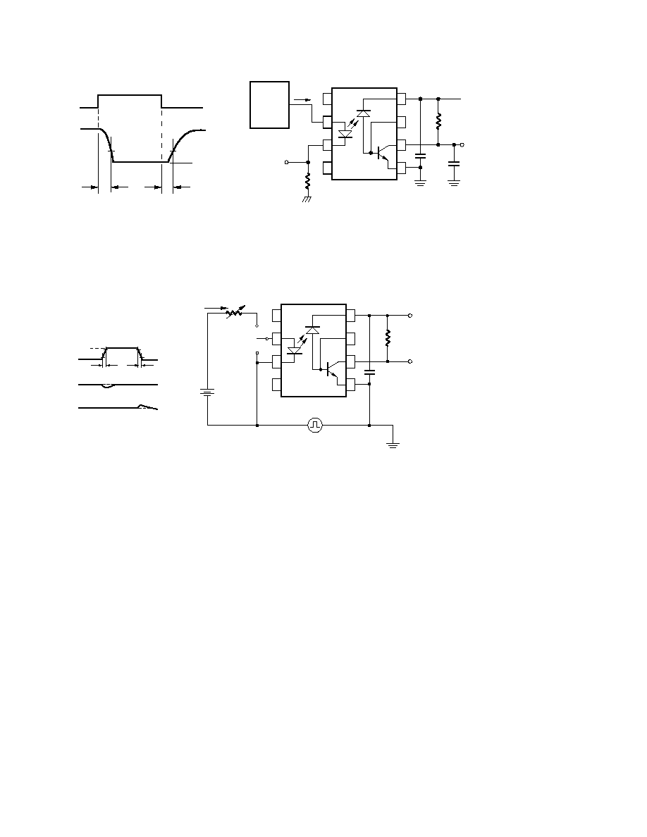
Figure 6. Test circuit for transient immunity and typical waveforms.
Figure 5. Switching test circuit.
O
V
3.3 V
OL
V
O
V
0 V
10%
90% 90%
10%
SWITCH AT A: I = 0 mA
F
SWITCH AT B: I = 16 mA
F
CM
V
t
r
t
f
7
1
2
3
4
5
6
8
V
O
0.1 µF
L
R
+3.3 V
PULSE GEN.
V
CM
+
≠
V
IF
*
A
B
FF
VO
PULSE
GEN.
Z = 50
t = 5 ns
O
r
I MONITOR
F
IF
0.1µF
L
R
CL = 1.5 µF
RM
0
tPHL
t
PLH
O
V
IF
OL
V
50%
+3.3 V
1
2
3
4
8
7
6
5
50%
10% DUTY CYCLE
1/f < 100 µS
10

www.agilent.com/semiconductors
For product information and a complete list of
distributors, please go to our web site.
For technical assistance call:
Americas/Canada: +1 (800) 235-0312 or
(916) 788-6763
Europe: +49 (0) 6441 92460
China: 10800 650 0017
Hong Kong: (+65) 6756 2394
India, Australia, New Zealand: (+65) 6755 1939
Japan: (+81 3) 3335-8152 (Domestic/Interna-
tional), or 0120-61-1280 (Domestic Only)
Korea: (+65) 6755 1989
Singapore, Malaysia, Vietnam, Thailand,
Philippines, Indonesia: (+65) 6755 2044
Taiwan: (+65) 6755 1843
Data subject to change.
Copyright © 2004 Agilent Technologies, Inc.
Obsoletes 5989-0300EN
December 20, 2004
5989-2111EN