 | ÐлекÑÑоннÑй компоненÑ: HCPL3140 | СкаÑаÑÑ:  PDF PDF  ZIP ZIP |
Äîêóìåíòàöèÿ è îïèñàíèÿ www.docs.chipfind.ru
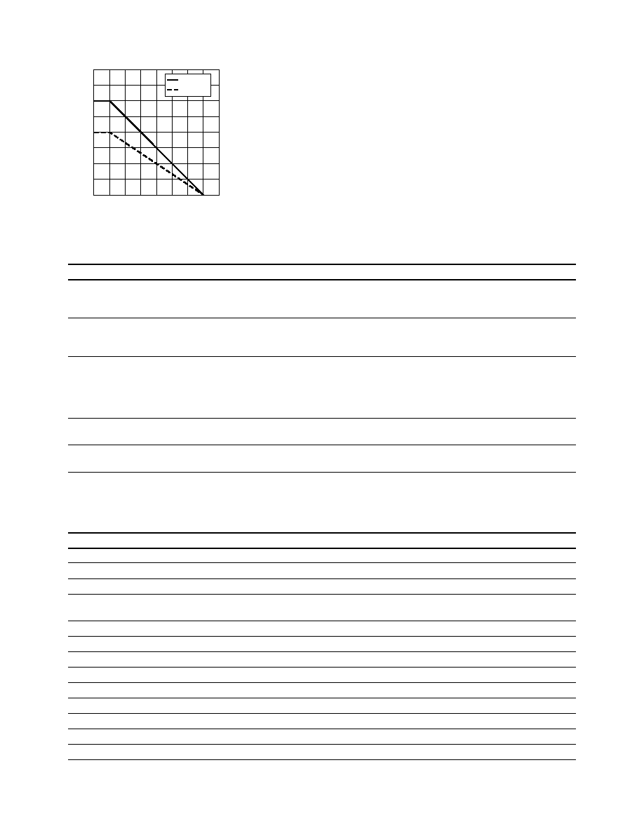
1
3
SHIELD
2
4
8
6
7
5
N/C
CATHODE
ANODE
N/C
V
CC
V
O
N.C.
V
EE
HCPL-3140/HCPL-0314
Agilent HCPL-3140/HCPL-0314
0.4 Amp Output Current IGBT
Gate Drive Optocoupler
Data Sheet
Features
· 0.4 A minimum peak output
current
· High speed response:
0.7
µ
s maximum propagation delay
over temperature range
· Ultra high CMR:
minimum 10 kV/
µ
s at V
CM
= 1 kV
· Bootstrappable supply current:
maximum 3 mA
· Wide operating temperature
range: 40
°
C to 100
°
C
· Wide V
CC
operating range:
10 V to 30 V over temp. range
· Available in DIP8 and SO8
package
· Safety approvals: UL approval
pending, 2500 V
rms
for 1 minute.
CSA approval pending. VDE
approval pending V
IORM
= 630 V
peak
(HCPL-3140)
Applications
·
Isolated IGBT/Power MOSFET
gate drive
·
AC and brushless DC motor drives
·
Inverters for home appliances
·
Industrial inverters
·
Switch Mode Power Supplies
(SMPS)
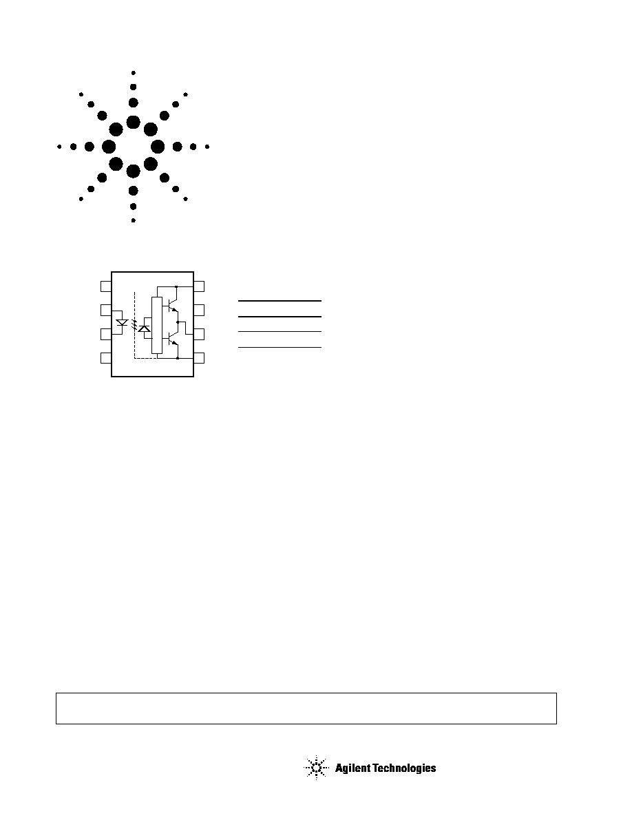
Truth Table
LED
V
O
OFF
LOW
ON
HIGH
A 0.1
µ
F bypass capacitor must be connected between pins V
CC
and V
EE
.
CAUTION: It is advised that normal static precautions be taken in handling and assembly of this component to prevent damage
and/or degradation which may be induced by ESD.
Description
The HCPL-3140/HCPL-0314
family of devices consists of a GaAsP LED
optically coupled to an integrated
circuit with a power output stage.
These optocouplers are ideally
suited for driving power IGBTs and
MOSFETs used in motor control
inverter applications. The high
operating voltage range of the
Functional Diagram
output stage provides the drive
voltages required by gate
controlled devices. The voltage
and current supplied by this
optocoupler makes it ideally
suited for directly driving small
or medium power IGBTs. For
IGBTs with higher ratings, the
HCPL-3150 (0.5 A) or
HCPL-3120 (2.0 A) optocouplers
can be used.
2
Ordering Information
Specify part number followed by option number (if desired).
Example :
HCPL-3140#XXX
No option = Standard DIP package, 50 per tube.
300 = Gull Wing Surface Mount Option, 50 per tube.
500 = Tape and Reel Packaging Option.
060 = VDE 0884, V
IORM
= 630 V
PEAK
.
HCPL-0314#XXX
No option = SOIC-8 surface mount in tube, 100 per tube.
500 = Tape and Reel Packaging Option.
060 = VDE 0884, V
IORM
= 566 V
PEAK
.
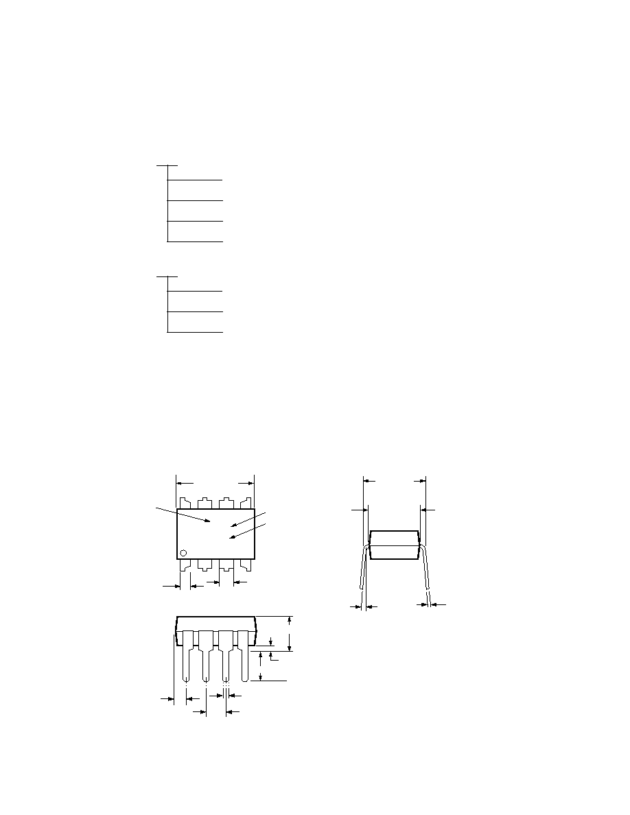
Package Outline Drawings
HCPL-3140 Standard DIP Package
9.65 ± 0.25
(0.380 ± 0.010)
1.78 (0.070) MAX.
1.19 (0.047) MAX.
A XXXXZ
YYWW
DATE CODE
1.080 ± 0.320
(0.043 ± 0.013)
2.54 ± 0.25
(0.100 ± 0.010)
0.51 (0.020) MIN.
0.65 (0.025) MAX.
4.70 (0.185) MAX.
2.92 (0.115) MIN.
DIMENSIONS IN MILLIMETERS AND (INCHES).
5
6
7
8
4
3
2
1
5° TYP.
OPTION CODE*
0.254
+ 0.076
- 0.051
(0.010
+ 0.003)
- 0.002)
7.62 ± 0.25
(0.300 ± 0.010)
6.35 ± 0.25
(0.250 ± 0.010)
TYPE NUMBER
* MARKING CODE LETTER FOR OPTION NUMBERS.
"V" = OPTION 060
OPTION NUMBERS 300 AND 500 NOT MARKED.
3
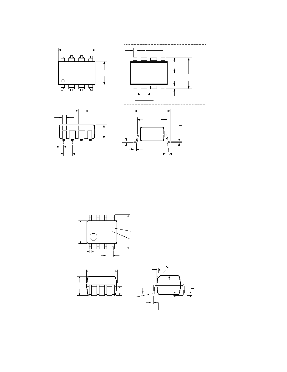
HCPL-0314 Small Outline SO-8 Package
XXX
YWW
8
7
6
5
4
3
2
1
5.994 ± 0.203
(0.236 ± 0.008)
3.937 ± 0.127
(0.155 ± 0.005)
0.406 ± 0.076
(0.016 ± 0.003)
1.270
(0.050)
BSG
5.080 ± 0.127
(0.200 ± 0.005)
3.175 ± 0.127
(0.125 ± 0.005)
1.524
(0.060)
45° X
0.432
(0.017)
0.228 ± 0.025
(0.009 ± 0.001)
TYPE NUMBER
(LAST 3 DIGITS)
DATE CODE
0.305
(0.012)
MIN.
TOTAL PACKAGE LENGTH (INCLUSIVE OF MOLD FLASH)
5.207 ± 0.254 (0.205 ± 0.010)
DIMENSIONS IN MILLIMETERS (INCHES).
LEAD COPLANARITY = 0.10 mm (0.004 INCHES) MAX.
0.203 ± 0.102
(0.008 ± 0.004)
7°
PIN ONE
0 ~ 7°
*
*
0.635 ± 0.25
(0.025 ± 0.010)
12° NOM.
9.65 ± 0.25
(0.380 ± 0.010)
0.635 ± 0.130
(0.025 ± 0.005)
7.62 ± 0.25
(0.300 ± 0.010)
5
6
7
8
4
3
2
1
9.65 ± 0.25
(0.380 ± 0.010)
6.350 ± 0.25
(0.250 ± 0.010)
1.016 (0.040)
1.194 (0.047)
1.194 (0.047)
1.778 (0.070)
9.398 (0.370)
9.906 (0.390)
4.826
(0.190)
TYP.
0.381 (0.015)
0.635 (0.025)
PAD LOCATION (FOR REFERENCE ONLY)
1.080 ± 0.320
(0.043 ± 0.013)
4.19
(0.165)
MAX.
1.780
(0.070)
MAX.
1.19
(0.047)
MAX.
2.54
(0.100)
BSC
DIMENSIONS IN MILLIMETERS (INCHES).
LEAD COPLANARITY = 0.10 mm (0.004 INCHES).
0.254
+ 0.076
- 0.051
(0.010
+ 0.003)
- 0.002)
HCPL-3140 Gull Wing Surface Mount Option 300 Outline Drawing
4
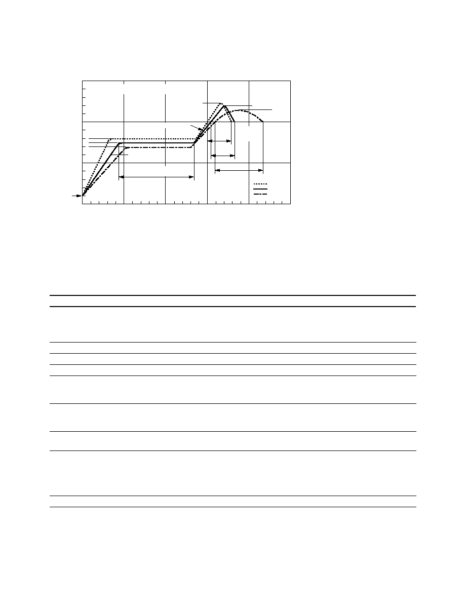
Solder Reflow Temperature Profile
Regulatory Information
The HCPL-3140/HCPL-0314 are
pending approval by the
following organizations:
VDE
Approval under VDE 0884/06.92
with V
IORM
= 630 V
peak
(HCPL-3140) and 566 V
peak
for
HCPL-0314.
UL
Approval under UL 1577,
component recognition program
up to V
ISO
= 2500 V
rms
expected
prior to product release. File
E55361.
CSA
Approval under CSA Component
Acceptance Notice #5, File CA
88324 expected prior to product
release.
VDE 0884 Insulation Characteristics (HCPL-3140 Option 060)
Description
Symbol
Characteristic
Unit
Installation classification per DIN VDE 0110/1.89, Table 1
for rated mains voltage
150 V
rms
I - IV
for rated mains voltage
300 V
rms
I - III
for rated mains voltage
600 V
rms
I-II
Climatic Classification
55/100/21
Pollution Degree (DIN VDE 0110/1.89)
2
Maximum Working Insulation Voltage
V
IORM
630
V
peak
Input to Output Test Voltage, Method b*
V
IORM
x 1.875=V
PR
, 100% Production Test with
V
PR
1181
V
peak
t
m
=1 sec, Partial discharge < 5 pC
Input to Output Test Voltage, Method a*
V
IORM
x 1.5=V
PR
, Type and Sample Test, t
m
=60 sec,
V
PR
945
V
peak
Partial discharge < 5 pC
Highest Allowable Overvoltage
V
IOTM
6000
V
peak
(Transient Overvoltage t
ini
= 10 sec)
Safety-limiting values - maximum values allowed in the
event of a failure.
Case Temperature
T
S
175
°
C
Input Current**
I
S,INPUT
230
mA
Output Power**
P
S, OUTPUT
600
mW
Insulation Resistance at T
S
, V
IO
= 500 V
R
S
>10
9
* Refer to the optocoupler section of the Isolation and Control Components Designer's Catalog, under Product Safety Regulations section, (VDE
0884) for a detailed description of Method a and Method b partial discharge test profiles.
** Refer to the following figure for dependence of P
S
and I
S
on ambient temperature.
0
TIME (SECONDS)
TEMPERATURE (°C)
200
100
50
150
100
200
250
300
0
30
SEC.
50 SEC.
30
SEC.
160°C
140°C
150°C
PEAK
TEMP.
245°C
PEAK
TEMP.
240°C
PEAK
TEMP.
230°C
SOLDERING
TIME
200°C
PREHEATING TIME
150°C, 90 + 30 SEC.
2.5°C ± 0.5°C/SEC.
3°C + 1°C/0.5°C
TIGHT
TYPICAL
LOOSE
ROOM
TEMPERATURE
PREHEATING RATE 3°C + 1°C/0.5°C/SEC.
REFLOW HEATING RATE 2.5°C ± 0.5°C/SEC.
5
OUTPUT POWER P
S
, INPUT CURRENT I
S
0
0
TS CASE TEMPERATURE °C
200
600
400
25
800
50
75 100
200
150 175
PS (mW)
125
100
300
500
700
IS (mA)
Insulation and Safety Related Specifications
Parameter
Symbol
HCPL-3140
HCPL-0314
Units
Conditions
Minimum External Air Gap
L(101)
7.1
4.9
mm
Measured from input terminals
(Clearance)
to output terminals, shortest
distance through air.
Minimum External Tracking
L(102)
7.4
4.8
mm
Measured from input terminals
(Creepage)
to output terminals, shortest
distance path along body.
Minimum Internal Plastic Gap
0.08
0.08
mm
Through insulation distance
(Internal Clearance)
conductor to conductor, usually
the straight line distance
thickness between the emitter
and detector.
Tracking Resistance
CTI
>175
>175
V
DIN IEC 112/VDE 0303 Part 1
(Comparative Tracking Index)
Isolation Group
IIIa
IIIa
Material Group (DIN VDE
0110, 1/89, Table 1)
Absolute Maximum Ratings
Parameter
Symbol
Min.
Max.
Units
Note
Storage Temperature
T
S
-55
125
°
C
Operating Temperature
T
A
-40
100
°
C
Average Input Current
I
F(AVG)
25
mA
1
Peak Transient Input Current (<1
µ
s pulse
I
F(TRAN)
1.0
A
width, 300pps)
Reverse Input Voltage
V
R
5
V
"High" Peak Output Current
I
OH(PEAK)
0.6
A
2
"Low" Peak Output Current
I
OL(PEAK)
0.6
A
2
Supply Voltage
V
CC
-V
EE
-0.5
35
V
Output Voltage
V
O(PEAK)
-0.5
V
CC
V
Output Power Dissipation
P
O
250
mW
3
Input Power Dissipation
P
I
105
mW
4
Lead Solder Temperature
260
°
C for 10 sec., 1.6 mm below seating plane
Solder Reflow Temperature Profile
See Package Outline Drawings section
Document Outline