 | –≠–ª–µ–∫—Ç—Ä–æ–Ω–Ω—ã–π –∫–æ–º–ø–æ–Ω–µ–Ω—Ç: HCPL-3150 | –°–∫–∞—á–∞—Ç—å:  PDF PDF  ZIP ZIP |
TRUTH TABLE
V
CC
- V
EE
V
CC
- V
EE
"Positive Going"
"Negative-Going"
LED
(i.e., Turn-On)
(i.e., Turn-Off)
V
O
OFF
0 - 30 V
0 - 30 V
LOW
ON
0 - 11 V
0 - 9.5 V
LOW
ON
11 - 13.5 V
9.5 - 12 V
TRANSITION
ON
13.5 - 30 V
12 - 30 V
HIGH
0.5 Amp Output Current IGBT
Gate Drive Optocoupler
Technical Data
HCPL-3150 (Single Channel)
HCPL-315J (Dual Channel)
Features
∑ 0.5 A Minimum Peak Output
Current
∑ 15 kV/
µ
s Minimum Common
Mode Rejection (CMR) at
V
CM
= 1500 V
∑ 1.0 V Maximum Low Level
Output Voltage (V
OL
)
Eliminates Need for
Negative Gate Drive
∑ I
CC
= 5 mA Maximum Supply
Current
∑ Under Voltage Lock-Out
Protection (UVLO) with
Hysteresis
∑ Wide Operating V
CC
Range:
15 to 30 Volts
∑ 0.5
µ
s Maximum
Propagation Delay
∑ +/≠ 0.35
µ
s Maximum Delay
Between Devices/Channels
∑ Industrial Temperature
Range:
-40
∞C to 100∞C
∑ HCPL-315J: Channel One to
Channel Two Output
Isolation = 1500 Vrms/1 min.
∑ Safety and Regulatory
Approval:
UL Recognized (UL1577)
3750 Vrms/1 min.
CAUTION: It is advised that normal static precautions be taken in handling and assembly of this component to
prevent damage and/or degradation which may be induced by ESD.
IEC/EN/DIN EN 60747-5-2
Approved
V
IORM
= 630 V
peak
(HCPL-3150 Option 060 only)
V
IORM
= 891 V
peak
(HCPL-
315J) CSA Certified
Applications
∑ Isolated IGBT/MOSFET
Gate Drive
∑ AC and Brushless DC Motor
Drives
∑ Industrial Inverters
∑ Switch Mode Power
Supplies (SMPS)
∑ Uninterruptable Power
Supplies (UPS)
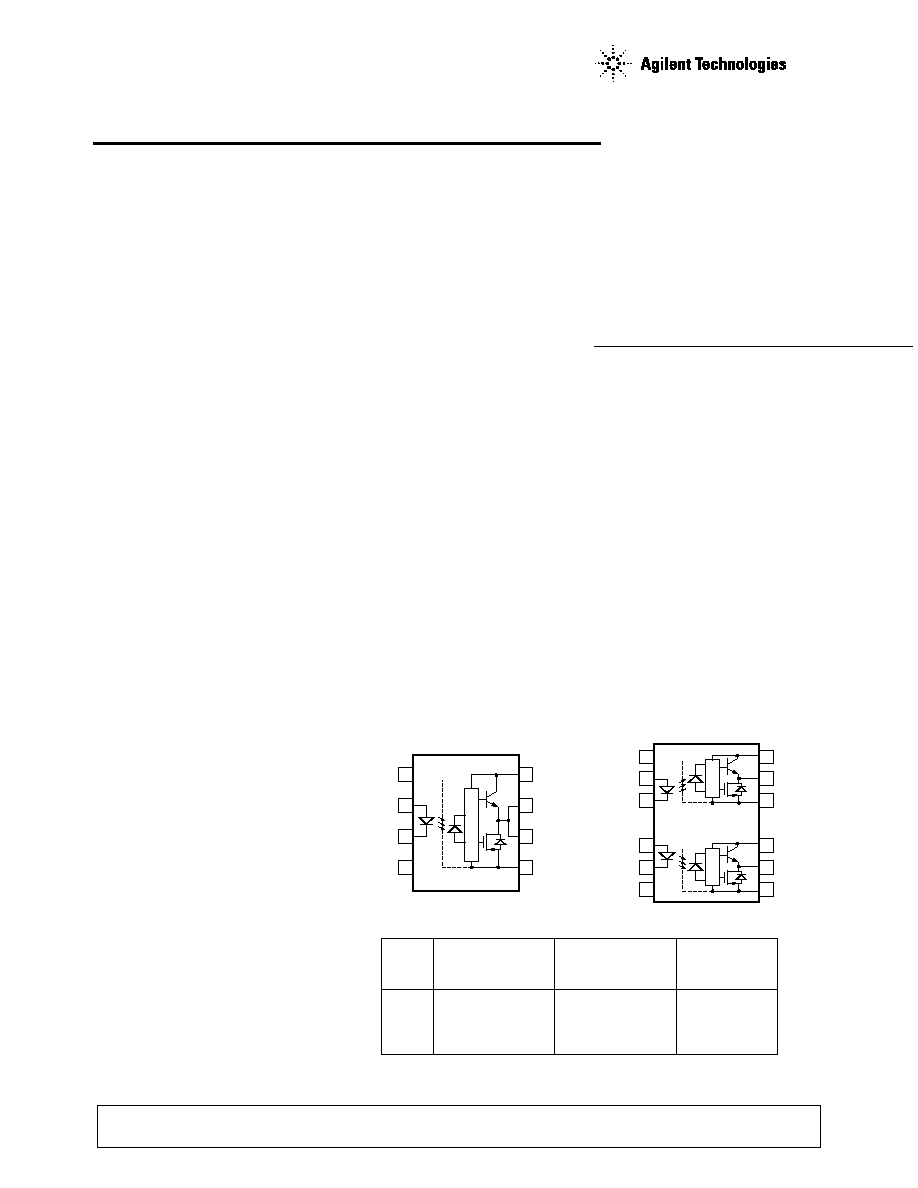
Description
The HCPL-315X consists of a
LED optically coupled to an
integrated circuit with a power
output stage. This optocoupler is
ideally suited for driving power
IGBTs and MOSFETs used in
motor control inverter applica-
tions. The high operating voltage
range of the output stage pro-
vides the drive voltages required
by gate controlled devices. The
voltage and current supplied by
this optocoupler makes it ideally
suited for directly driving IGBTs
with ratings up to 1200 V/50 A.
For IGBTs with higher ratings,
the HCPL-3150/315J can be used
to drive a discrete power stage
which drives the IGBT gate.
A 0.1
µF bypass capacitor must be connected between the V
CC
and V
EE
pins for each channel.
Functional Diagram
1
3
SHIELD
2
4
8
6
7
5
N/C
CATHODE
ANODE
N/C
V
CC
V
O
V
O
V
EE
HCPL-3150
1
3
SHIELD
2
8
16
14
15
9
N/C
CATHODE
ANODE
N/C
V
CC
V
EE
V
O
V
EE
7
6
10
11
CATHODE
ANODE
V
O
V
CC
SHIELD
HCPL-315J
2
Ordering Information
Specify Part Number followed by Option Number (if desired)
Example
HCPL-315Y#XXXX
No Option = Standard DIP package, 50 per tube.
060 = IEC/EN/DIN EN 60747-5-2 V
IORM
= 630 Vpeak Option, 50 per tube.
(HCPL-3150 only)
300 = Gull Wing Surface Mount Option, 50 per tube. (HCPL-3150 only)
500 = Tape and Reel Packaging Option.
HCPL-3150; 1000 per reel.
HCPL-315J; 850 per reel.
XXXE = Lead Free Option
= Single Channel, 8-pin PDIP.
J = Dual Channel, SO16.
Option data sheets available. Contact Agilent sales representative or authorized distributor.
Remarks: The notation "#" is used for existing products, while (new) products launched since 15th July 2001 and lead free option will use "≠"
Package Outline Drawings
Standard DIP Package
Selection Guide: Invertor Gate Drive Optoisolators
Widebody
Package Type
8-Pin DIP (300 mil)
(400 mil)
Small Outline SO-16
Part Number
HCPL-3150
HCPL-3120
HCPL-J312
HCPL-J314
HCNW-3120
HCPL-315J
HCPL-316J
HCPL-314J
Number of
1
1
1
1
1
2
1
2
Channels
IEC/EN/DIN EN
V
IORM
V
IORM
V
IORM
V
IORM
60747-5-2
630 V
peak
891V
peak
1414 V
peak
891 V
peak
Approvals
Option 060
UL
3750
3750
5000
3750
Approval
Vrms/1 min.
Vrms/1 min.
Vrms/1min.
Vrms/1 min.
Output Peak
0.5A
2A
2A
0.4A
2A
0.5A
2A
0.4A
Current
CMR
15 kV/
µs
10 kV/
µs
15 kV/
µs
10 kV/
µs
(minimum)
UVLO
Yes
No
Yes
No
Fault Status
No
Yes
No
9.40 (0.370)
9.90 (0.390)
PIN ONE
1.78 (0.070) MAX.
1.19 (0.047) MAX.
A 3150 Z
YYWW
DATE CODE
0.76 (0.030)
1.40 (0.055)
2.28 (0.090)
2.80 (0.110)
0.51 (0.020) MIN.
0.65 (0.025) MAX.
4.70 (0.185) MAX.
2.92 (0.115) MIN.
6.10 (0.240)
6.60 (0.260)
0.20 (0.008)
0.33 (0.013)
5∞ TYP.
7.36 (0.290)
7.88 (0.310)
1
2
3
4
8
7
6
5
5
6
7
8
4
3
2
1
GND1
V
DD1
V
IN+
V
IN≠
GND2
V
DD2
V
OUT+
V
OUT≠
PIN DIAGRAM
PIN ONE
DIMENSIONS IN MILLIMETERS AND (INCHES).
* MARKING CODE LETTER FOR OPTION NUMBERS.
"V" = OPTION 060.
OPTION NUMBERS 300 AND 500 NOT MARKED.
OPTION CODE*
NOTE: FLOATING LEAD PROTRUSION IS 0.25 mm (10 mils) MAX.
3.56 ± 0.13
(0.140 ± 0.005)
3
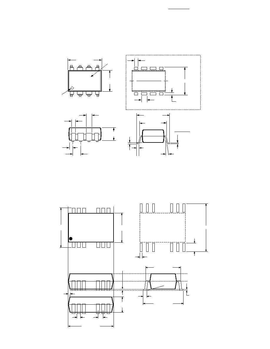
Package Outline Drawings
Gull-Wing Surface-Mount Option 300
16 - Lead Surface Mount
0.635 ± 0.25
(0.025 ± 0.010)
12∞ NOM.
0.20 (0.008)
0.33 (0.013)
9.65 ± 0.25
(0.380 ± 0.010)
0.635 ± 0.130
(0.025 ± 0.005)
7.62 ± 0.25
(0.300 ± 0.010)
5
6
7
8
4
3
2
1
9.65 ± 0.25
(0.380 ± 0.010)
6.350 ± 0.25
(0.250 ± 0.010)
MOLDED
1.080 ± 0.320
(0.043 ± 0.013)
1.780
(0.070)
MAX.
1.19
(0.047)
MAX.
2.540
(0.100)
BSC
DIMENSIONS IN MILLIMETERS (INCHES).
TOLERANCES (UNLESS OTHERWISE SPECIFIED):
LEAD COPLANARITY
MAXIMUM: 0.102 (0.004)
xx.xx = 0.01
xx.xxx = 0.005
A 3150 Z
YYWW
*MARKING CODE LETTER FOR OPTION
NUMBERS.
"V" = OPTION 060.
OPTION NUMBERS 300 AND 500 NOT MARKED.
OPTION
CODE*
1.016 (0.040)
1.27 (0.050)
10.9 (0.430)
2.0 (0.080)
LAND PATTERN RECOMMENDATION
3.56 ± 0.13
(0.140 ± 0.005)
NOTE: FLOATING LEAD PROTRUSION IS 0.25 mm (10 mils) MAX.
HCPL-315J
10.36 ± 0.20
(0.408 ± 0.008)
(0.295 ± 0.004)
7.49 ± 0.10
(0.406 ± 0.007)
10.31 ± 0.18
(0.138 ± 0.005)
3.51 ± 0.13
(0.018)
0.457
(0.050)
1.27
9∞
16 15 14
11 10
9
1
2
3
6
7
8
VIEW
FROM
PIN 16
VIEW
FROM
PIN 1
(0.025 MIN.)
0.64
(0.408 ± 0.008)
10.36 ± 0.20
(0.0091 ≠ 0.0125)
0.23 ≠ 0.32
(0.345 ± 0.008)
8.76 ± 0.20
ALL LEADS TO BE COPLANAR ± (0.002 INCHES) 0.05 mm.
DIMENSIONS IN (INCHES) AND MILLIMETERS.
0 - 8∞
V
CC1
V
O1
GND
1
V
CC2
V
O2
GND
2
NC
V
IN1
V
1
V
IN2
V
2
NC
(0.004 ≠ 0.011)
0.10 ≠ 0.30
STANDOFF
NOTE: FLOATING LEAD PROTRUSION IS 0.25 mm (10 mils) MAX.
(0.458) 11.63
(0.085) 2.16
(0.025) 0.64
LAND PATTERN RECOMMENDATION

4
Regulatory Information
The HCPL-3150 and HCPL-315J
have been approved by the
following organizations:
UL
Recognized under UL 1577,
Component Recognition
Program, File E55361.
CSA
Approved under CSA Component
Acceptance Notice #5, File CA
88324.
IEC/EN/DIN EN 60747-5-2
Approved under:
IEC 60747-5-2:1997 + A1:2002
EN 60747-5-2:2001 + A1:2002
DIN EN 60747-5-2 (VDE 0884
Teil 2):2003-01.
(Option 060 and HCPL-315J only)
Solder Reflow Thermal Profile
0
TIME (SECONDS)
TEMPERATURE (
∞
C)
200
100
50
150
100
200
250
300
0
30
SEC.
50 SEC.
30
SEC.
160∞C
140∞C
150∞C
PEAK
TEMP.
245∞C
PEAK
TEMP.
240∞C
PEAK
TEMP.
230∞C
SOLDERING
TIME
200∞C
PREHEATING TIME
150∞C, 90 + 30 SEC.
2.5∞C ± 0.5∞C/SEC.
3∞C + 1∞C/≠0.5∞C
TIGHT
TYPICAL
LOOSE
ROOM
TEMPERATURE
PREHEATING RATE 3∞C + 1∞C/≠0.5∞C/SEC.
REFLOW HEATING RATE 2.5∞C ± 0.5∞C/SEC.
Recommended Pb-Free IR Profile
217 ∞C
RAMP-DOWN
6 ∞C/SEC. MAX.
RAMP-UP
3 ∞C/SEC. MAX.
150 - 200 ∞C
260 +0/-5 ∞C
t 25 ∞C to PEAK
60 to 150 SEC.
20-40 SEC.
TIME WITHIN 5 ∞C of ACTUAL
PEAK TEMPERATURE
tp
ts
PREHEAT
60 to 180 SEC.
tL
TL
Tsmax
Tsmin
25
Tp
TIME
TEMPERA
TURE
NOTES:
THE TIME FROM 25 ∞C to PEAK TEMPERATURE = 8 MINUTES MAX.
Tsmax = 200 ∞C, Tsmin = 150 ∞C
5
IEC/EN/DIN EN 60747-5-2
Insulation Characteristics
Description
Symbol
HCPL-3150#060
HCPL-315J**
Unit
Installation classification per DIN VDE
0110/1.89, Table 1
for rated mains voltage
150 Vrms
I-IV
for rated mains voltage
300 Vrms
I-IV
I-III
for rated mains voltage
600 Vrms
I-III
I-II
Climatic Classification
55/100/21
55/100/21
Pollution Degree (DIN VDE 0110/1.89)
2
2
Maximum Working Insulation Voltage
V
IORM
630
891
Vpeak
Input to Output Test Voltage, Method b*
V
IORM
x 1.875 = V
PR
, 100% Production
Test with t
m
= 1 sec,
V
PR
1181
1670
Vpeak
Partial discharge < 5 pC
Input to Output Test Voltage, Method a*
V
IORM
x 1.5 = V
PR
, Type and Sample
Test, t
m
= 60 sec,
V
PR
945
1336
Vpeak
Partial discharge < 5 pC
Highest Allowable Overvoltage*
V
IOTM
6000
6000
Vpeak
(Transient Overvoltage t
ini
= 10 sec)
Safety-Limiting Values ≠ Maximum Values
Allowed in the Event of a Failure, Also
See Figure 37, Thermal Derating Curve.
Case Temperature
T
S
175
175
∞C
Input Current
I
S, INPUT
230
400
mA
Output Power
P
S, OUTPUT
600
1200
mW
Insulation Resistance at T
S
, V
IO
= 500 V
R
S
10
9
10
9
**Approval Pending.
*Refer to the front of the optocoupler section of the current Catalog, under Product Safety Regulations section IEC/EN/DIN EN
60747-5-2, for a detailed description of Method a and Method b partial discharge test profiles.
Note: Isolation characteristics are guaranteed only within the safety maximum ratings which must be ensured by protective circuits
in application.