 | –≠–ª–µ–∫—Ç—Ä–æ–Ω–Ω—ã–π –∫–æ–º–ø–æ–Ω–µ–Ω—Ç: HCPL-3160 | –°–∫–∞—á–∞—Ç—å:  PDF PDF  ZIP ZIP |

1-212
H
2.0 Amp IGBT Gate Drive
Optocoupler with Integrated
Over-current Protection and
Fault Feedback
Preliminary Technical Data
Features
∑ Integrated IGBT
Desaturation Protection
∑ Integrated Optically Isolated
IGBT Fault Status Feedback
∑ CMOS Compatible INPUT
and FAULT Status Indicator
∑ Small Printed Circuit Board
Footprint (SO-16 Package)
∑ -40
∞
C to 100
∞
C Operating
Temperature
∑ Suitable for Integration in
Power Modules
∑ 2.0 A Minimum Peak Output
Current
∑ 15 kV/
µ
s Minimum Common
Mode Rejection (CMR) at
V
CM
= 1500 V
∑ V
IORM
= 890 V
PEAK
HCPL-3160
Description
The HCPL-3160 provides low cost,
area efficient IGBT gate drive
that includes desaturation or over
current detection and local IGBT
shutdown. The integrated fault
feedback optocoupler notifies
the controller when the IGBT is
shutdown due to a desaturation
or over current condition.
This data sheet represents the latest information at the time of publication of this catalog. All specifications
subject to change. Samples available Fall 1996.
16
15
14
13
12
11
10
9
1
2
3
4
5
6
7
8
SHIELD
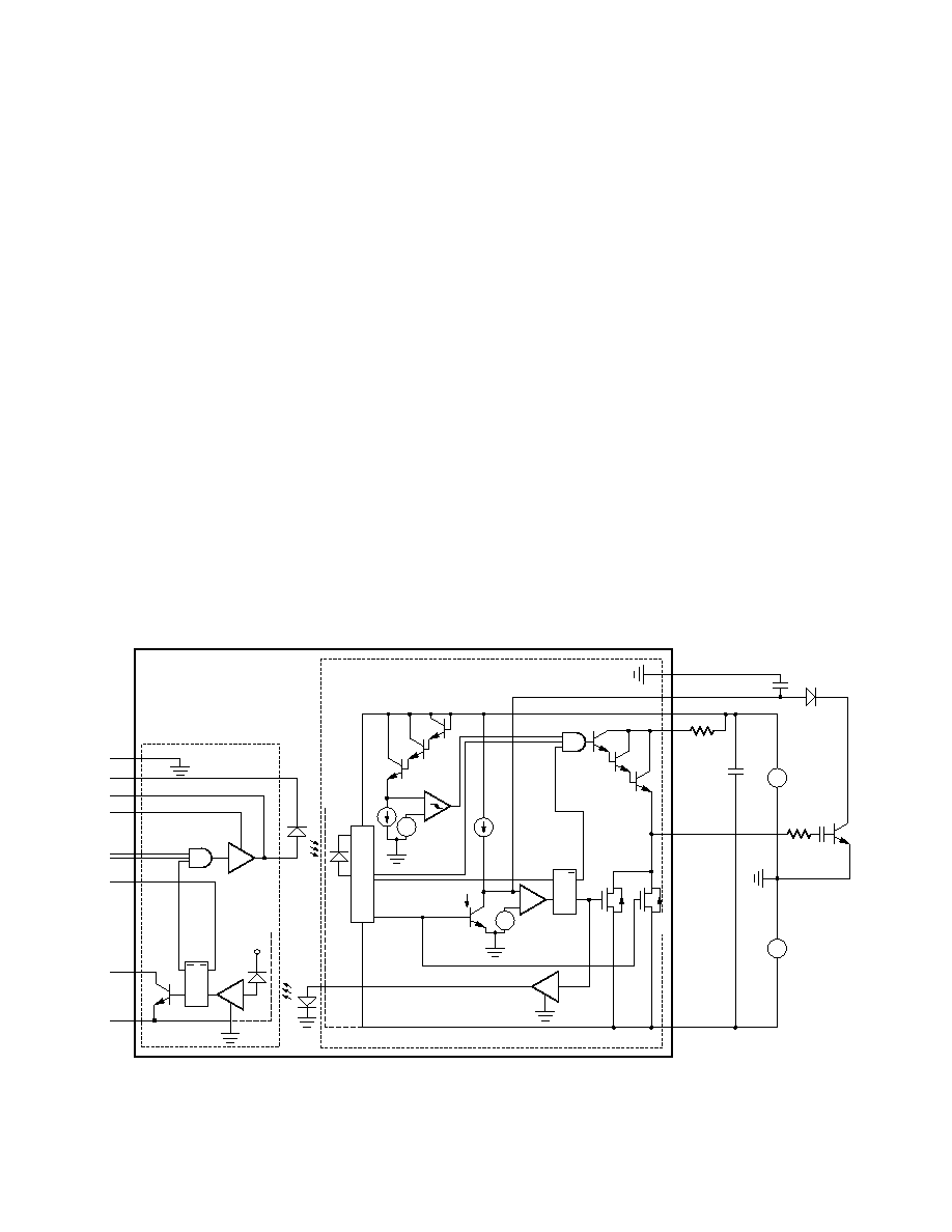
Functional Diagram
HP 3160
9630
Actual Size
1-213
Fault Circuit Operation
A typical desaturation protected
IGBT gate drive application
circuit using the HCPL-3160 is
shown in Figure 1. The IGBT
collector to emitter voltage
is monitored through D
DESAT
.
When the IGPT is on and V
DESAT
exceeds the internal reference
voltage of 7 V the IGBT gate is
"softly" turned-off by M2 to
prevent large di/dt generation.
The LED2 driver is also activated,
which drives the internal
feedback LED2 and notifies the
controller of the IGBT fault by
bringing the FAULT output low.
The FAULT output remains
low until RESET is brought low.
(Note if a separate reset line
is not required, RESET can be
connected to Vin on the circuit
board. In this case, the FAULT
output will be reset on the next
PWM cycle that Vin goes low.)
The FAULT output is an open
collector which allows the FAULT
outputs from all the HCPL-3160s
in a drive to be connected
together in a "wired OR" forming
V
CC1
Q R
Q S
SHIELD
GND
FAULT
RESET
V
IN
ENABLE
V
CC1
LED1+
LED1≠
GND
BUFFER IC
LED1
R Q
S Q
D
R
I
V
E
R
≠
+
+
≠
+
≠
+
≠
+
≠
V
CC2
+
≠
V
EE
0.1 µF
V
E
D
DESAT
V
E
R
G
C
BLANK
TRIPLE
DARLINGTON
UVLO
I
CHG
I
DSCHG
Q1
V
E
V
E
7 V
DESAT
M2
1X
V
E
V
UVLO
12 V/11 V
V
E
LED2
SHIELD
R
2
(OPTIONAL)
M1
33X
A3
LED2
DRIVER
DETECTOR IC
HCPL-3160
LIGHTGUIDE 1
LIGHTGUIDE 2
Figure 1. IGBT Gate Drive with Desaturation Protection and Fault Feedback.
a single fault bus for interfacing
with the micro-controller. The
ENABLE input can also be
connected to this fault bus. With
this connection all IGBTs in a
drive are shutdown without
micro-controller intervention
once a fault is detected on a
single IGBT.
C
BLANK
disables the fault
detection circuitry for a time
period sufficient for normal IGBT
turn-on. C
BLANK
is held low by
Q1 when the IGBT is off.

1-214
Parameter
Symbol
Min.
Typ.*
Max.
Units
Conditions
Logic Low
INPUT
0.8
V
Voltages
RESET
FAULT
ENABLE
Logic High
INPUT
2.0
V
Voltages
RESET
FAULT
ENABLE
High Level
I
OH
0.5
1.5
A
V
O
= V
CC2
-4 V
Output Current
2.0
A
V
O
= V
CC2
15 V
Low Level
I
OL
0.5
2.0
A
V
O
= V
EE
+ 2.5 V
Output Current
2.0
A
V
O
= V
EE
+ 15
High Level
V
OH
V
CC2
-4 V
CC2
-3
V
I
O
= -100 mA
Output Voltage
Low Level
V
OL
0.1
0.5
V
I
O
= 100 mA
Output Voltage
High Level Supply
I
CC1H
12
mA
Vin = 5 V, V
CC1
= 5 V
Current
High Level
I
CC1L
2
mA
Vin = 0 V, V
CC1
= 5 V
Supply Current
High Level
I
CC2H
3
7
mA
output open
Supply Current
Low Level
I
CC2L
3
7
mA
output open
Supply Current
Blanking Capacitor
I
CHG
0.2
0.32
0.45
mA
Vdesat = 0 V
Charging Current
Blanking Capacitor
I
DSCHG
60
mA
Vdesat = 7 V
Discharge Current
UVLO Threshold
V
UVLO+
13.0
13.4
V
V
CC2
= 1.0 ms ramp,
(10.9) (12.5)
V
O
> 5 V
V
UVLO-
11.2
11.6
V
V
CC2
= 1.0 ms ramp,
(8.7)
(9.5)
V
O
> 5 V
UVLO Hysteresis
V
UVLO+ -
1.4
V
V
UVLO-
Desaturation Trip
V
DESAT
6.0
7.0
8.0
V
Voltage
Preliminary Electrical Specifications (DC)
Over recommended operating conditions (T
A
= -40 to 100
∞
C) unless otherwise specified.
*All typical values at T
A
= 25
∞
C and V
CC2
- V
EE
= 30 V, unless otherwise noted.
1)
V
UVLO+
and V
UVLO-
are specified as the V
CC2
at which V
O
exceeds 5 V. The approximate output voltage just prior/after the UVLO
transition is given in parenthesis.

1-215
Parameter Symbol
Min.
Typ.*
Max.
Units
Conditions
Propagation Delay Time
t
PLH
0.10
0.30
0.50
µ
s
Rg = 10
,
to High Output Level
Cg = 10 nF,
Propagation Delay Time
t
PHL
0.10
0.50
µ
s
f = 10 kHz, Duty Cycle = 50%
to Low Output Level
Pulse Width Distortion
pwd
-0.1
0.1
µ
s
Propagation Delay
t
PHL
- t
PLH
-0.4
0.4
µ
s
Difference Between
Any Two Parts
Rise Time
t
r
0.1
µ
s
Fall Time
t
f
0.1
µ
s
Propagation Delay
t
P(DS)
1.5
µ
s
Rg = 10
,
Time from Desat to
CG = 10 nF
Low Level Output
Propagation Delay
t
PF(DS)
10
µ
s
RG = 10
,
Time from Desat to
CG = 10 nF
Low Level FAULT Signal
Minimum FAULT
t
FAULT
2.0
µ
s
Signal Pulse Width
UVLO Turn Off Delay
t
UVLO OFF
0.6
µ
s
Output High Level
|CM
H
|
15
30
kV/
µ
s
T
A
= 25
∞
C, INPUT = 5 V,
Common Mode
V
CM
= 1500 V, V
CC
= 30 V
Transient Immunity
Output Low Level
|CM
L
|
15
30
kV/
µ
s
T
A
= 25
∞
C, V
CM
= 1500 V,
Common Mode
INPUT = 0 V, V
CC2
= 30 V
Transient Immunity
Preliminary Switching Specifications (AC)
Over recommended operating conditions (T
A
= -40 to 100
∞
C) unless otherwise specified.
*All typical values at T
A
= 25
∞
C and V
CC2
- V
EE
= 30 V, unless otherwise noted.