1-361
H
Optically Coupled 20 mA
Current Loop Transmitter
Technical Data
HCPL-4100
Features
∑ Guaranteed 20 mA Loop
Parameters
∑ Data Input Compatible with
LSTTL, TTL and CMOS
Logic
∑ Guaranteed Performance
over Temperature (0
∞
C to
70
∞
C)
∑ Internal Shield for High
Common Mode Rejection
∑ 20 kBaud Data Rate at 400
Metres Line Length
∑ Guaranteed On and Off
Output Current Levels
∑ Safety Approval
UL Recognized -2500 V rms for
1 minute
CSA Approved
∑ Optically Coupled 20 mA
Current Loop Receiver,
HCPL-4200, Also Available
Applications
∑ Isolated 20 mA Current
Loop Transmitter in:
Computer Peripherals
Industrial Control Equipment
Data Communications
Equipment
Description
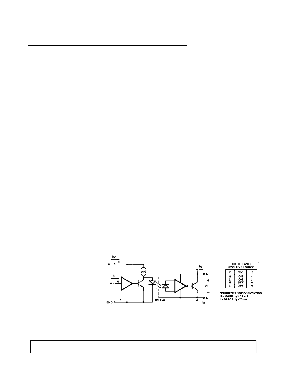
The HCPL-4100 optocoupler is
designed to operate as a transmit-
ter in equipment using the 20 mA
current loop. 20 mA current loop
systems conventionally signal a
logic high state by transmitting
20 mA of loop current (MARK),
and signal a logic low state by
allowing no more than a few
milliamperes of loop current
(SPACE). Optical coupling of the
signal from the logic input to the
20 mA current loop breaks
ground loops and provides very
high immunity to common mode
interference.
The HCPL-4100 data input is
compatible with LSTTL, TTL, or
CMOS logic gates. The input
integrated circuit drives a GaAsP
LED. The light emitted by the
LED is sensed by a second inte-
grated circuit that allows 20 mA
to pass with a voltage drop of less
than 2.7 volts when no light is
emitted and allows less than 2 mA
to pass when light is emitted. The
transmitter output is capable of
withstanding 27 volts. The input
integrated circuit provides a
controlled amount of LED drive
current and takes into account
any LED light output degrada-
tion. The internal shield allows a
guaranteed 1000 V/
µ
s common
mode transient immunity.
CAUTION: It is advised that normal static precautions be taken in handling and assembly of this component to
prevent damage and/or degradation which may be induced by ESD.
Functional Diagram
A 0.1
µ
F bypass capacitor connected between pins 8 and 5 is recommended.
5965-3581E
1-363
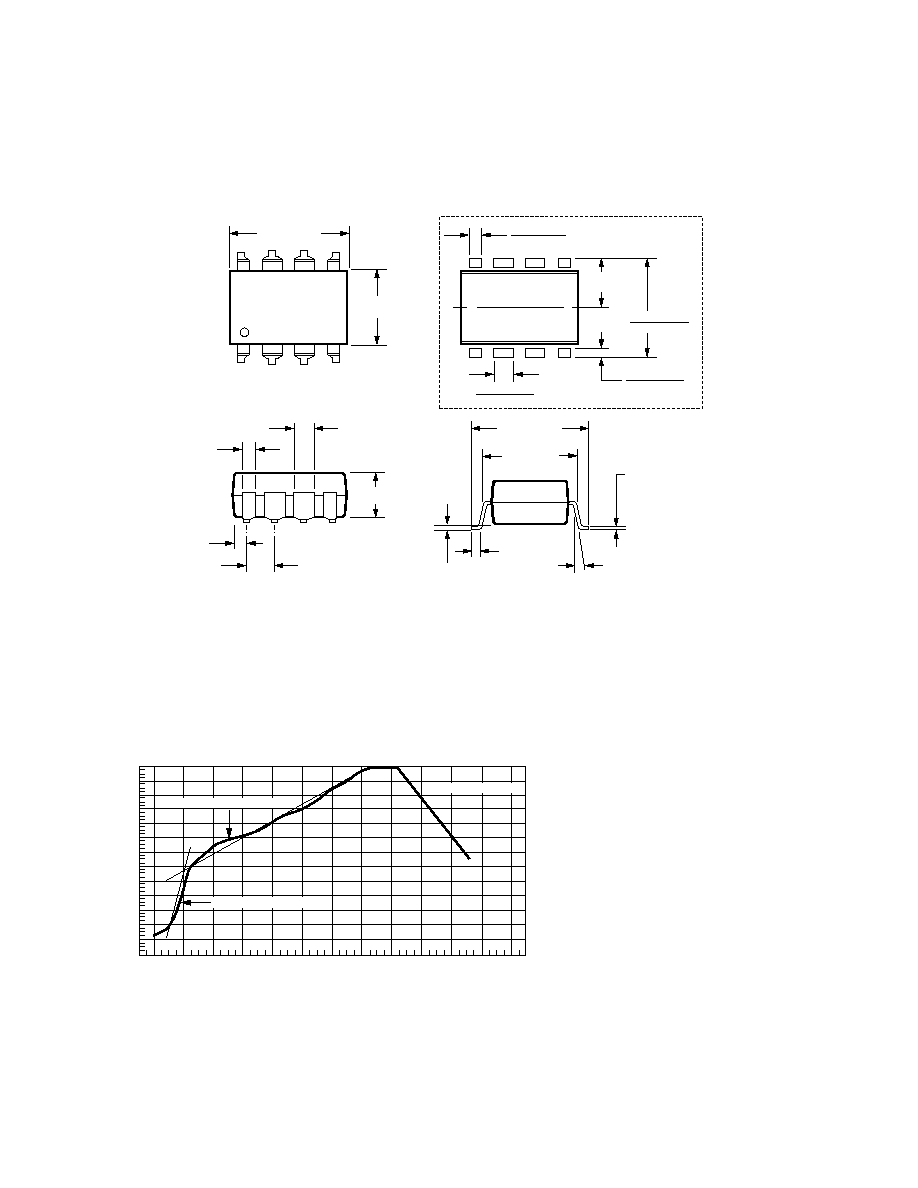
8-Pin DIP Package with Gull Wing Surface Mount Option 300 (HCPL-4100)
240
T = 115∞C, 0.3∞C/SEC
0
T = 100∞C, 1.5∞C/SEC
T = 145∞C, 1∞C/SEC
TIME ≠ MINUTES
TEMPERATURE ≠ ∞C
220
200
180
160
140
120
100
80
60
40
20
0
260
1
2
3
4
5
6
7
8
9
10
11
12
Thermal Profile (Option #300)
Figure 1. Maximum Solder Reflow Thermal Profile.
(Note: Use of non-chlorine activated fluxes is recommended.)
0.635 ± 0.25
(0.025 ± 0.010)
12∞ NOM.
9.65 ± 0.25
(0.380 ± 0.010)
0.635 ± 0.130
(0.025 ± 0.005)
7.62 ± 0.25
(0.300 ± 0.010)
5
6
7
8
4
3
2
1
9.65 ± 0.25
(0.380 ± 0.010)
6.350 ± 0.25
(0.250 ± 0.010)
1.016 (0.040)
1.194 (0.047)
1.194 (0.047)
1.778 (0.070)
9.398 (0.370)
9.906 (0.390)
4.826
(0.190)
TYP.
0.381 (0.015)
0.635 (0.025)
PAD LOCATION (FOR REFERENCE ONLY)
1.080 ± 0.320
(0.043 ± 0.013)
4.19
(0.165)
MAX.
1.780
(0.070)
MAX.
1.19
(0.047)
MAX.
2.54
(0.100)
BSC
DIMENSIONS IN MILLIMETERS (INCHES).
LEAD COPLANARITY = 0.10 mm (0.004 INCHES).
0.254
+ 0.076
- 0.051
(0.010
+ 0.003)
- 0.002)
1-364
Regulatory Information
The HCPL-4100 has been
approved by the following
organizations:
UL
Recognized under UL 1577,
Component Recognition
Program, File E55361.
CSA
Approved under CSA Component
Acceptance Notice #5, File CA
88324.
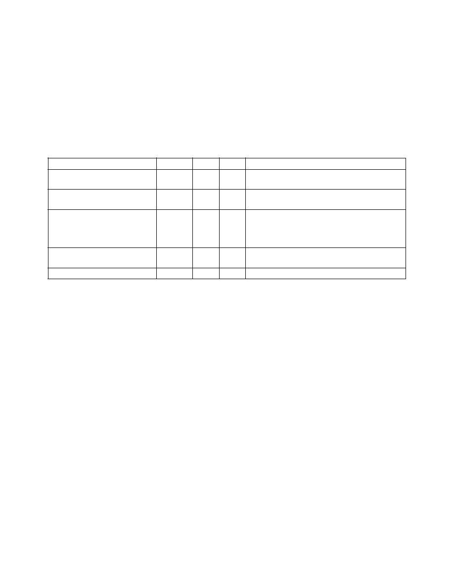
Insulation and Safety Related Specifications
Parameter
Symbol
Value
Units
Conditions
Min. External Air Gap
L(IO1)
7.1
mm
Measured from input terminals to output
(External Clearance)
terminals, shortest distance through air
Min. External Tracking Path
L(IO2)
7.4
mm
Measured from input terminals to output
(External Creepage)
terminals, shortest distance path along body
Min. Internal Plastic Gap
0.08
mm
Through insulation distance, conductor to
(Internal Clearance)
conductor, usually the direct distance
between the photoemitter and photodetector
inside the optocoupler cavity
Tracking Resistance
CTI
200
Volts
DIN IEC 112/VDE 0303 PART 1
(Comparative Tracking Index)
Isolation Group
IIIa
Material Group (DIN VDE 0110, 1/89, Table 1)
Option 300 ≠ surface mount classification is Class A in accordance with CECC 00802.
Absolute Maximum Ratings
(No Derating Required up to 55
∞
C)
Storage Temperature .................................................. -55
∞
C to +125
∞
C
Operating Temperature ................................................. -40
∞
C to +85
∞
C
Lead Solder Temperature .... 260
∞
C for 10 s (1.6 mm below seating plane)
Supply Voltage ≠ V
CC
.............................................................. 0 V to 20 V
Average Output Current - I
O
........................................ -30 mA to 30 mA
Peak Output Current - I
O
........................................... Internally Limited
Output Voltage ≠ V
O
........................................................ -0.4 V to 27 V
Input Voltage ≠ V
I
............................................................ -0.5 V to 20 V
Input Power Dissipation ≠ P
I
................................................. 265 mW
[1]
Output Power Dissipation ≠ P
O
............................................. 125 mW
[2]
Total Power Dissipation ≠ P .................................................. 360 mW
[3]
Infrared and Vapor Phase Reflow Temperature
(Option #300) .......................................... see Fig. 1, Thermal Profile

