Document Outline
- Selector Guide
- List of Figures
- 1. Maximum Solder Reflow Thermal Profile.
- 2. Typical Output Voltage vs. Loop Current.
- 3. Typical Current Switching Threshold vs. Temperature.
- 4. Typical Input Loop Voltage vs. Input Current.
- 5. Typical Input Voltage vs. Temperature.
- 6. Typical Logic Low Output Voltage vs. Temperature.
- 7. Typical Logic High Output Current vs. Temperature.
- 8. Test Circuit for t PHL , t PLH , t r , and t f .
- 9. Waveforms for t PHL , t PLH , t r , and t f .
- 10. Typical Propagation Delay vs. Temperature.
- 11. Typical Rise, Fall Time vs. Temperature.
- 12. Test Circuit for t PZH , t PZL , t PHZ , and t PLZ .
- 13. Waveforms for t PZH , t PZL , t PHZ , and t PLZ .
- 14. Typical Logic High Enable Propagation Delay vs. Temperature.
- 15. Typical Logic Low Enable Propagation Delay vs. Temperature.
- 16. Test Circuit for Common Mode Transient Immunity.
- 17. Simplex Current Loop System Configurations for (a) Point-to-Point, (b) Multidrop.
- 18. Recommended Non-Isolated Active Transmitter with HCPL-4200 Isolated Receiver for Simplex Point-to-Point 20 mA Current
- 19. Minimum Required Supply Voltage, V CC , vs. Loop Length for Current Loop Circuit of Figure 19.
- 20. Typical Data Rate vs. Distance.
- 21. Full Duplex Point-to-Point Current Loop System Configuration.
- 22. Half Duplex Current Loop System Configurations for (a) Point-to-Point, (b) Multidrop.
- Features
- Applications
- Description
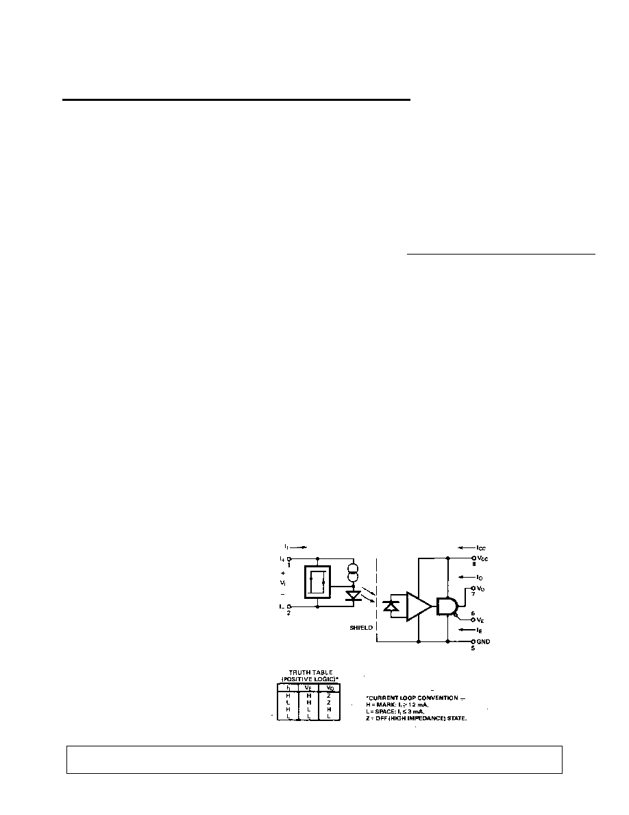
- Functional Diagram
- Ordering Information
- Package Outline Drawings
- Thermal Profile (Option #300)
- Regulatory Information
- Insulation and Safety Related Specifications
- Absolute Maximum Ratings
- Recommended Operating Conditions
- DC Electrical Specifications
- Switching Specifications
- Package Characteristics
- Applications
1-373
H
Optically Coupled 20 mA
Current Loop Receiver
Technical Data
HCPL-4200
Features
� Data Output Compatible
with LSTTL, TTL and CMOS
� 20 K Baud Data Rate at 1400
Metres Line Length
� Guaranteed Performance
over Temperature (0
�
C to
70
�
C)
� Guaranteed On and Off
Thresholds
� LED is Protected from
Excess Current
� Input Threshold Hysteresis
� Three-State Output Compat-
ible with Data Buses
� Internal Shield for High
Common Mode Rejection
� Safety Approval
UL Recognized -2500 V rms,
for 1 Minute
CSA Approved
� Optically Coupled 20 mA
Current Loop Transmitter,
HCPL-4100, Also Available
Applications
� Isolated 20 mA Current
� Loop Receiver in:
Computer Peripherals
Industrial Control Equipment
Data Communications
Equipment
Description
The HCPL-4200 optocoupler is
designed to operate as a receiver
in equipment using the 20 mA
Current Loop. 20 mA current
loop systems conventionally sig-
nal a logic high state by transmit-
ting 20 mA of loop current
(MARK), and signal a logic low
state by allowing no more than a
few milliamperes of loop current
(SPACE). Optical coupling of the
signal from the 20 mA current
loop to the logic output breaks
ground loops and provides for a
very high common mode
rejection. The HCPL-4200 aids in
the design process by providing
guaranteed thresholds for logic
high state and logic low state for
the current loop, providing an
LSTTL, TTL, or CMOS compatible
logic interface, and providing
guaranteed common mode
rejection. The buffer circuit on
the current loop side of the
HCPL-4200 provides typically 0.8
mA of hysteresis which increases
the immunity to common mode
and differential mode noise. The
buffer also provides a controlled
amount of LED drive current
which takes into account any
LED light output degradation.
The internal shield allows a
guaranteed 1000 V/
�
s common
mode transient immunity.
CAUTION: It is advised that normal static precautions be taken in handling and assembly of this component to
prevent damage and/or degradation which may be induced by ESD.
Functional Diagram
A 0.1
�
F bypass capacitor connected between pins 8 and 5 is recommended.
5965-3580E
1-374
Ordering Information
Specify part number followed by Option Number (if desired).
HCPL-4200# XXX
300 = Gull Wing Surface Mount Lead Option
500 = Tape/Reel Package Option (1 K min)
Option data sheets available. Contact your Hewlett-Packard sales representative or authorized distributor for
information.
Package Outline Drawings �
8 Pin DIP Package (HCPL-4200)
8 Pin DIP Package with Gull Wing Surface Mount Option 300 (HCPL-4200)
0.635 � 0.25
(0.025 � 0.010)
12� NOM.
9.65 � 0.25
(0.380 � 0.010)
0.635 � 0.130
(0.025 � 0.005)
7.62 � 0.25
(0.300 � 0.010)
5
6
7
8
4
3
2
1
9.65 � 0.25
(0.380 � 0.010)
6.350 � 0.25
(0.250 � 0.010)
1.016 (0.040)
1.194 (0.047)
1.194 (0.047)
1.778 (0.070)
9.398 (0.370)
9.906 (0.390)
4.826
(0.190)
TYP.
0.381 (0.015)
0.635 (0.025)
PAD LOCATION (FOR REFERENCE ONLY)
1.080 � 0.320
(0.043 � 0.013)
4.19
(0.165)
MAX.
1.780
(0.070)
MAX.
1.19
(0.047)
MAX.
2.54
(0.100)
BSC
DIMENSIONS IN MILLIMETERS (INCHES).
LEAD COPLANARITY = 0.10 mm (0.004 INCHES).
0.254
+ 0.076
- 0.051
(0.010
+ 0.003)
- 0.002)
9.65 � 0.25
(0.380 � 0.010)
1.78 (0.070) MAX.
1.19 (0.047) MAX.
HP XXXX
YYWW
DATE CODE
1.080 � 0.320
(0.043 � 0.013)
2.54 � 0.25
(0.100 � 0.010)
0.51 (0.020) MIN.
0.65 (0.025) MAX.
4.70 (0.185) MAX.
2.92 (0.115) MIN.
DIMENSIONS IN MILLIMETERS AND (INCHES).
5
6
7
8
4
3
2
1
5� TYP.
TYPE NUMBER
UL
RECOGNITION
UR
0.254
+ 0.076
- 0.051
(0.010
+ 0.003)
- 0.002)
7.62 � 0.25
(0.300 � 0.010)
6.35 � 0.25
(0.250 � 0.010)
1-375
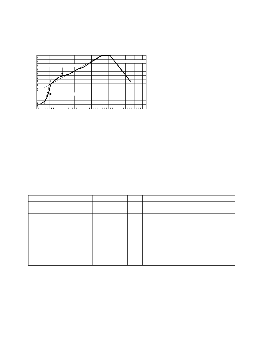
Thermal Profile (Option #300)
240
T = 115�C, 0.3�C/SEC
0
T = 100�C, 1.5�C/SEC
T = 145�C, 1�C/SEC
TIME � MINUTES
TEMPERATURE � �C
220
200
180
160
140
120
100
80
60
40
20
0
260
1
2
3
4
5
6
7
8
9
10
11
12
Figure 1. Maximum Solder Reflow Thermal Profile.
(Note: Use of non-chlorine activated fluxes is recommended.)
Regulatory Information
The HCPL-4200 has been
approved by the following
organizations:
UL
Recognized under UL 1577,
Component Recognition
Program, File E55361.
CSA
Approved under CSA Component
Acceptance Notice #5, File CA
88324.
Insulation and Safety Related Specifications
Parameter
Symbol
Value
Units
Conditions
Min. External Air Gap
L(IO1)
7.1
mm
Measured from input terminals to output
(External Clearance)
terminals, shortest distance through air
Min. External Tracking Path
L(IO2)
7.4
mm
Measured from input terminals to output
(External Creepage)
terminals, shortest distance path along body
Min. Internal Plastic Gap
0.08
mm
Through insulation distance, conductor to
(Internal Clearance)
conductor, usually the direct distance
between the photoemitter and photodetector
inside the optocoupler cavity
Tracking Resistance
CTI
200
volts
DIN IEC 112/VDE 0303 PART 1
(Comparative Tracking Index)
Isolation Group
IIIa
Material Group (DIN VDE 0110, 1/89, Table 1)
Option 300 � surface mount classification is Class A in accordance with CECC 00802.
1-376
Absolute Maximum Ratings
(No Derating Required up to 70
�
C)
Storage Temperature .................................................. -55
�
C to +125
�
C
Operating Temperature ................................................. -40
�
C to +85
�
C
Lead Solder Temperature .... 260
�
C for 10 s (1.6 mm below seating plane)
Supply Voltage � V
CC
.............................................................. 0 V to 20 V
Average Input Current - I
I
........................................... -30 mA to 30 mA
Peak Transient Input Current - I
I
............................................... 0.5 A
[1]
Enable Input Voltage � V
E
................................................ -0.5 V to 20 V
Output Voltage � V
O
........................................................ -0.5 V to 20 V
Average Output Current � I
O
....................................................... 25 mA
Input Power Dissipation � P
I
................................................... 90 mW
[2]
Output Power Dissipation � P
O
............................................. 210 mW
[3]
Total Power Dissipation � P .................................................. 255 mW
[4]
Infrared and Vapor Phase Reflow Temperature
(Option #300) .......................................... see Fig. 1, Thermal Profile
Recommended Operating Conditions
Parameter
Symbol
Min.
Max.
Units
Power Supply Voltage
V
CC
4.5
20
Volts
Forward Input Current
I
SI
0
2.0
mA
(SPACE)
Forward Input Current
I
MI
14
24
mA
(MARK)
Operating Temperature
T
A
0
70
�
C
Fan Out
N
0
4
TTL Loads
Logic Low Enable
V
EL
0
0.8
Volts
Voltage
Logic High Enable
V
EH
2.0
20
Volts
Voltage
1-377
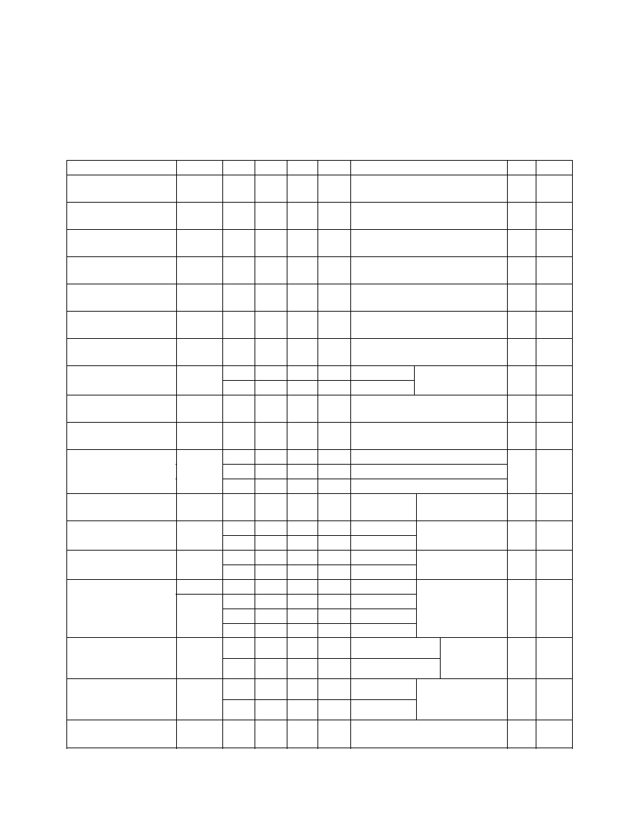
DC Electrical Specifications
For 0
�
C
T
A
70
�
C, 4.5 V
V
CC
20 V, V
E
= 0.8 V, all typicals at T
A
= 25
�
C and V
CC
= 5 V unless otherwise
noted. See note 13.
Parameter
Symbol
Min. Typ. Max. Units
Test Conditions
Fig.
Note
Mark State Input
I
MI
12
mA
2, 3,
Current
4
Mark State Input
V
MI
2.52
2.75
Volts
I
I
= 20 mA
V
E
= Don't Care
4, 5
Voltage
Space State Input
I
SI
3
mA
2, 3,
Current
4
Space State Input
V
SI
1.6
2.2
Volts
I
I
= 0.5 to 2.0 mA
V
E
= Don't
2, 4
Voltage
Care
Input Hysteresis
I
HYS
0.3
0.8
mA
2
Current
Logic Low Output
V
OL
0.5
Volts
I
OL
= 6.4 mA
I
I
= 3 mA
6
Voltage
(4 TTL Loads)
Logic High Output
V
OH
2.4
Volts
I
OH
= -2.6 mA,
I
I
= 12 mA
7
Voltage
Output Leakage
I
OHH
100
�
A
V
O
= 5.5 V
I
I
= 20 mA
500
�
A
V
O
= 20 V
Logic High Enable
V
EH
2.0
Volts
Voltage
Logic Low Enable
V
EL
0.8
Volts
Voltage
Logic High Enable
I
EH
20
�
A
V
E
= 2.7 V
100
�
A
V
E
= 5.5 V
0.004 250
�
A
V
E
= 20 V
Logic Low Enable
I
EL
-0.32
mA
V
E
= 0.4 V
Current
Logic Low Supply
I
CCL
4.5
6.0
mA
V
CC
= 5.5 V
I
I
= 0 mA
5.25
7.5
mA
V
CC
= 20 V
Logic High Supply
I
CCH
2.7
4.5
mA
V
CC
= 5.5 V
I
I
= 20 mA
3.1
6.0
mA
V
CC
= 20 V
High Impedance
I
OZL
-20
�
A
V
O
= 0.4 V
V
E
= 2 V,
I
OZH
20
�
A
V
O
= 2.4 V
100
�
A
V
O
= 5.5 V
500
�
A
V
O
= 20 V
Logic Low Short
I
OSL
25
mA
V
O
= V
CC
= 5.5 V
I
I
= 0 mA
5
40
mA
V
O
= V
CC
= 20 V
Logic High Short
I
OSH
-10
mA
V
CC
= 5.5 V
I
I
= 20 mA
5
-25
mA
V
CC
= 20 V
Input Capacitance
C
IN
120
pF
f = 1 MHz, V
I
= 0 V dc,
Pins 1 and 2
Current (V
OUT
> V
CC
)
Current
Current
State Output
Current
Current
Circuit Output
Current
Circuit Output
Current
I
I
= 20 mA
V
O
= GND
V
CC
= 4.5 V
V
E
= Don't Care
V
E
= Don't Care