
Intelligent Power Module
and Gate Drive Interface
Optocouplers
Technical Data
Features
∑ Performance Specified for
Common IPM Applications
over Industrial Temperature
Range: -40
∞
C to 100
∞
C
∑ Fast Maximum Propagation
Delays
t
PHL
= 480 ns
t
PLH
= 550 ns
∑ Minimized Pulse Width
Distortion
PWD = 450 ns
∑ 15 kV/
µ
s Minimum Common
Mode Transient Immunity
at V
CM
= 1500 V
∑ CTR > 44% at I
F
= 10 mA
∑ Safety Approval
UL Recognized
-2500 V rms / 1 min. for
HCPL-4506/0466
-3750 V rms / 1 min. for
HCPL-J456
-5000 V rms / 1 min. for
HCPL-4506 Option 020
and HCNW4506
CSA Approved
VDE0884 Approved
-V
IORM
= 560 Vpeak for
HCPL-0466 Option 060
-V
IORM
= 630 Vpeak for
HCPL-4506 Option 060
-V
IORM
= 891 Vpeak for
HCPL-J456
-V
IORM
= 1414 Vpeak for
HCNW4506
The connection of a 0.1
µ
F bypass capacitor between pins 5 and 8 is recommended.
Applications
∑ IPM Isolation
∑ Isolated IGBT/MOSFET Gate
Drive
∑ AC and Brushless DC Motor
Drives
∑ Industrial Inverters
HCPL-4506
HCPL-J456
HCPL-0466
HCNW4506
CAUTION: It is advised that normal static precautions be taken in handling and assembly of this component to
prevent damage and/or degradation which may be induced by ESD.
Functional Diagram
Truth Table
LED
V
O
ON
L
OFF
H
8
7
6
1
3
SHIELD
5
2
4
20 k
NC
ANODE
CATHODE
NC
VCC
VL
VO
GND

2
Selection Guide
Standard
White Mold
Package
8-Pin DIP
8-Pin DIP
Small Outline
Widebody
Type
(300 Mil)
(300 Mil)
SO8
(400 Mil)
Hermetic*
Part
HCPL-4506
HCPL-J456
HCPL-0466
HCNW4506
HCPL-5300
Number
HCPL-5301
VDE0884
V
IORM
= 630 Vpeak V
IORM
= 891 Vpeak V
IORM
= 560 Vpeak V
IORM
= 1414 Vpeak
--
Approval
(Option 060)
(Option 060)
*Technical data for these products are on separate Agilent publications.
Ordering Information
Specify Part Number followed by Option Number (if desired).
Example:
HCPL-4506#XXX
020 = UL 5000 V rms/1 minute Option** for HCPL-4506 Only.
060 = VDE0884 Option** for HCPL-4506/0466.
300 = Gull Wing Lead Option for HCPL-4506/J456, HCNW4506.
500 = Tape and Reel Packaging Option
Option data sheets are available. Contact Agilent sales representative or authorized distributor
for information.
**Combination of Option 020 and Option 060 is not available.
Description
The HCPL-4506 and HCPL-0466
contain a GaAsP LED while the
HCPL-J456 and the HCNW4506
contain an AlGaAs LED. The LED
is optically coupled to an inte-
grated high gain photo detector.
Minimized propagation delay
difference between devices makes
these optocouplers excellent
solutions for improving inverter
efficiency through reduced
switching dead time.
An on chip 20 k
output pull-up
resistor can be enabled by
shorting output pins 6 and 7, thus
eliminating the need for an
external pull-up resistor in
common IPM applications.
Specifications and performance
plots are given for typical IPM
applications.

3
Package Outline Drawings
HCPL-4506 and HCPL-J456 Outline Drawing
0.635 ± 0.25
(0.025 ± 0.010)
12∞ NOM.
9.65 ± 0.25
(0.380 ± 0.010)
0.635 ± 0.130
(0.025 ± 0.005)
7.62 ± 0.25
(0.300 ± 0.010)
5
6
7
8
4
3
2
1
9.65 ± 0.25
(0.380 ± 0.010)
6.350 ± 0.25
(0.250 ± 0.010)
1.016 (0.040)
1.194 (0.047)
1.194 (0.047)
1.778 (0.070)
9.398 (0.370)
9.906 (0.390)
4.826
(0.190)
TYP.
0.381 (0.015)
0.635 (0.025)
PAD LOCATION (FOR REFERENCE ONLY)
1.080 ± 0.320
(0.043 ± 0.013)
4.19
(0.165)
MAX.
1.780
(0.070)
MAX.
1.19
(0.047)
MAX.
2.54
(0.100)
BSC
DIMENSIONS IN MILLIMETERS (INCHES).
LEAD COPLANARITY = 0.10 mm (0.004 INCHES).
0.254
+ 0.076
- 0.051
(0.010
+ 0.003)
- 0.002)
HCPL-4506 and HCPL-J456 Gull Wing Surface Mount Option 300 Outline Drawing
9.65 ± 0.25
(0.380 ± 0.010)
1.78 (0.070) MAX.
1.19 (0.047) MAX.
A XXXXZ
YYWW
DATE CODE
1.080 ± 0.320
(0.043 ± 0.013)
2.54 ± 0.25
(0.100 ± 0.010)
0.51 (0.020) MIN.
0.65 (0.025) MAX.
4.70 (0.185) MAX.
2.92 (0.115) MIN.
DIMENSIONS IN MILLIMETERS AND (INCHES).
5
6
7
8
4
3
2
1
5∞ TYP.
OPTION CODE*
UL
RECOGNITION
UR
0.254
+ 0.076
- 0.051
(0.010
+ 0.003)
- 0.002)
7.62 ± 0.25
(0.300 ± 0.010)
6.35 ± 0.25
(0.250 ± 0.010)
TYPE NUMBER
* MARKING CODE LETTER FOR OPTION NUMBERS (HCPL-4506).
"L" = OPTION 020
"V" = OPTION 060
OPTION NUMBERS 300 AND 500 NOT MARKED.

4
HCPL-0466 Outline Drawing (8-Pin Small Outline Package)
HCNW4506 Outline Drawing (8-Pin Widebody Package)
XXX
YWW
8
7
6
5
4
3
2
1
5.994 ± 0.203
(0.236 ± 0.008)
3.937 ± 0.127
(0.155 ± 0.005)
0.406 ± 0.076
(0.016 ± 0.003)
1.270
(0.050)
BSG
5.080 ± 0.127
(0.200 ± 0.005)
3.175 ± 0.127
(0.125 ± 0.005)
1.524
(0.060)
45∞ X
0.432
(0.017)
0.228 ± 0.025
(0.009 ± 0.001)
TYPE NUMBER
(LAST 3 DIGITS)
DATE CODE
0.305
(0.012)
MIN.
TOTAL PACKAGE LENGTH (INCLUSIVE OF MOLD FLASH)
5.207 ± 0.254 (0.205 ± 0.010)
DIMENSIONS IN MILLIMETERS (INCHES).
LEAD COPLANARITY = 0.10 mm (0.004 INCHES) MAX.
0.203 ± 0.102
(0.008 ± 0.004)
7∞
PIN ONE
0 ~ 7∞
*
*
5
6
7
8
4
3
2
1
11.15 ± 0.15
(0.442 ± 0.006)
1.78 ± 0.15
(0.070 ± 0.006)
5.10
(0.201)
MAX.
1.55
(0.061)
MAX.
2.54 (0.100)
TYP.
DIMENSIONS IN MILLIMETERS (INCHES).
7∞ TYP.
0.254
+ 0.076
- 0.0051
(0.010
+ 0.003)
- 0.002)
11.00
(0.433)
9.00 ± 0.15
(0.354 ± 0.006)
MAX.
10.16 (0.400)
TYP.
A
HCNWXXXX
YYWW
DATE CODE
TYPE NUMBER
0.51 (0.021) MIN.
0.40 (0.016)
0.56 (0.022)
3.10 (0.122)
3.90 (0.154)
5
Note: Use of nonchlorine activated fluxes is recommended.
Solder Reflow Temperature Profile
1.00 ± 0.15
(0.039 ± 0.006)
7∞ NOM.
12.30 ± 0.30
(0.484 ± 0.012)
0.75 ± 0.25
(0.030 ± 0.010)
11.00
(0.433)
5
6
7
8
4
3
2
1
11.15 ± 0.15
(0.442 ± 0.006)
9.00 ± 0.15
(0.354 ± 0.006)
1.3
(0.051)
12.30 ± 0.30
(0.484 ± 0.012)
6.15
(0.242)TYP.
0.9
(0.035)
PAD LOCATION (FOR REFERENCE ONLY)
1.78 ± 0.15
(0.070 ± 0.006)
4.00
(0.158)
MAX.
1.55
(0.061)
MAX.
2.54
(0.100)
BSC
DIMENSIONS IN MILLIMETERS (INCHES).
LEAD COPLANARITY = 0.10 mm (0.004 INCHES).
0.254
+ 0.076
- 0.0051
(0.010
+ 0.003)
- 0.002)
MAX.
240
T = 115∞C, 0.3∞C/SEC
0
T = 100∞C, 1.5∞C/SEC
T = 145∞C, 1∞C/SEC
TIME ≠ MINUTES
TEMPERATURE ≠ ∞C
220
200
180
160
140
120
100
80
60
40
20
0
260
1
2
3
4
5
6
7
8
9
10
11
12
HCNW4506 Gull Wing Surface Mount Option 300 Outline Drawing

6
Insulation and Safety Related Specifications
Value
Parameter
Symbol HCPL-4506 HCPL-J456 HCPL-0466 HCNW4506 Units
Conditions
Minimum External
L(101)
7.1
7.4
4.9
9.6
mm
Measured from input
Air Gap (External
terminals to output
Clearance)
terminals, shortest
distance through air.
Minimum External
L(102)
7.4
8.0
4.8
10.0
mm
Measured from input
Tracking (External
terminals to output
Creepage)
terminals, shortest
distance path along body.
Minimum Internal
0.08
0.5
0.08
1.0
mm
Through insulation
Plastic Gap
distance, conductor to
(Internal Clearance)
conductor, usually the
direct distance between
the photoemitter and
photodetector inside the
optocoupler cavity.
Minimum Internal
NA
NA
NA
4.0
mm
Measured from input
Tracking (Internal
terminals to output
Creepage)
terminals, along internal
cavity.
Tracking Resistance
CTI
175
175
175
200
Volts
DIN IEC 112/VDE 0303
(Comparative
Part 1
Tracing Index)
Isolation Group
IIIa
IIIa
IIIa
IIIa
Material Group (DIN
VDE 0110, 1/89, Table 1)
Regulatory Information
The devices contained in this data sheet have been approved by the following agencies:
Agency/Standard
HCPL-4506
HCPL-J456
HCPL-0466 HCNW4506
Underwriters Laboratories (UL)
UL 1577
Recognized under UL 1577, Component
Recognized Program, Category FPQU2,
File E55361
Canadian Standards
Component
Association (CSA)
Acceptance
File CA88324
Notice #5
Verband Deutscher
DIN VDE 0884
Electrotechniker (VDE)
(June 1992)
Technischer
DIN VDE 0884
Uberwachungs-Verein
(June 1992)
Rheinland (TUV) Certificate R9650938
All Agilent data sheets report the creepage and clearance inherent to the optocoupler component itself. These
dimensions are needed as a starting point for the equipment designer when determining the circuit insulation require-
ments. However, once mounted on a printed circuit board, minimum creepage and clearance requirements must be
met as specified for individual equipment standards. For creepage, the shortest distance path along the surface of a
printed circuit board between the solder fillets of the input and output leads must be considered. There are recom-
mended techniques such as grooves and ribs which may be used on a printed circuit board to achieve desired creepage
and clearances. Creepage and clearance distances will also change depending on factors such as pollution degree and
insulation level.

7
VDE 0884 Insulation Related Characteristics
HCPL-0466 HCPL-4506
Description
Symbol Option 060 Option 060 HCPL-J456 HCNW4506 Unit
Installation classification per
DIN VDE 0110/1.89, Table 1
for rated mains voltage
150 V rms
I-IV
I-IV
I-IV
I-IV
for rated mains voltage
300 V rms
I-III
I-IV
I-IV
I-IV
for rated mains voltage
450 V rms
I-III
I-III
I-IV
for rated mains voltage
600 V rms
I-III
I-IV
for rated mains voltage
1000 V rms
I-III
Climatic Classification
55/100/21
55/100/21
55/100/21
55/100/21
Pollution Degree
2
2
2
2
(DIN VDE 0110/1.89)
Maximum Working
V
IORM
560
630
891
1414
V
peak
Insulation Voltage
Input to Output Test Voltage,
Method b* V
IORM
x 1.875 = V
PR
,
100% Production Test with t
m
=
V
PR
1050
1181
1670
2652
V
peak
1 sec, Partial Discharge < 5pC
Input to Output Test Voltage,
Method a* V
IORM
x 1.5 = V
PR
,
Type and Sample Test, t
m
= 60 sec,
V
PR
840
945
1336
2121
V
peak
Partial Discharge < 5pC
Highest Allowable Overvoltage*
V
IOTM
4000
6000
6000
8000
V
peak
(Transient Overvoltage, t
ini
= 10 sec)
Safety Limiting Values ≠ maximum
values allowed in the event of a fail-
ure, also see Thermal Derating curve.
Case Temperature
T
S
150
175
175
150
∞
C
Input Current
I
S INPUT
150
230
400
400
mA
Output Power
P
S OUTPUT
600
600
600
700
mW
Insulation Resistance at T
S
,
R
S
10
9
10
9
10
9
10
9
V
IO
= 500 V
*Refer to the optocoupler section of the Designer's Catalog, under regulatory information (VDE 0884) for a detailed description of
Method a and Method b partial discharge test profiles.
Note: These optocouplers are suitable for "safe electrical isolation" only within the safety limit data. Maintenance of the safety data
shall be ensured by means of protective circuits.
Note: Insulation Characteristics are per DIN VDE 0884 (June 1992 revision).
Note: Surface mount classification is Class A in accordance with CECC 00802.

8
Absolute Maximum Ratings
Parameter
Symbol
Min.
Max.
Units
Storage Temperature
T
S
-55
125
∞
C
Operating Temperature
T
A
-40
100
∞
C
Average Input Current
[1]
I
F(avg)
25
mA
Peak Input Current
[2]
(50% duty cycle,
1 ms pulse width)
I
F(peak)
50
mA
Peak Transient Input Current (<1
µ
s pulse width, 300 pps)
I
F(tran)
1.0
A
Reverse Input Voltage (Pin 3-2)
HCPL-4506, HCPL-0466
V
R
5
Volts
HCPL-J456, HCNW4506
3
Average Output Current (Pin 6)
I
O(avg)
15
mA
Resistor Voltage (Pin 7)
V
7
-0.5
V
CC
Volts
Output Voltage (Pin 6-5)
V
O
-0.5
30
Volts
Supply Voltage (Pin 8-5)
V
CC
-0.5
30
Volts
Output Power Dissipation
[3]
P
O
100
mW
Total Power Dissipation
[4]
P
T
145
mW
Lead Solder Temperature (HCPL-4506, HCPL-J456)
260
∞
C for 10 s, 1.6 mm below seating plane
Lead Solder Temperature (HCNW4506)
260
∞
C for 10 s
(up to seating plane)
Infrared and Vapor Phase Reflow Temperature
See Package Outline Drawings Section
(HCPL-0466 and Option 300)
Recommended Operating Conditions
Parameter
Symbol
Min.
Max.
Units
Power Supply Voltage
V
CC
4.5
30
Volts
Output Voltage
V
O
0
30
Volts
Input Current (ON)
I
F(on)
10
20
mA
Input Voltage (OFF)
V
F(off)
*
-5
0.8
V
Operating Temperature
T
A
-40
100
∞
C
*Recommended V
F(OFF)
= -3 V to 0.8 V for HCPL-J456, HCNW4506.

9
Electrical Specifications
Over recommended operating conditions unless otherwise specified:
T
A
= -40
∞
C to +100
∞
C, V
CC
= +4.5 V to 30 V, I
F(on)
= 10 mA to 20 mA, V
F(off)
= -5 V to 0.8 V
Parameter
Symbol
Device
Min. Typ.* Max. Units Test Conditions Fig. Note
Current Transfer Ratio
CTR
44
90
%
I
F
= 10 mA,
5
V
O
= 0.6 V
Low Level Output Current
I
OL
4.4
9.0
mA
I
F
= 10 mA,
1, 2
V
O
= 0.6 V
Low Level Output Voltage
V
OL
0.3
0.6
V
I
O
= 2.4 mA
Input Threshold Current
I
TH
HCPL-4506
1.5
5
mA
V
O
= 0.8 V,
1
16
HCPL-0466
I
O
= 0.75 mA
HCNW4506
HCPL-J456
0.6
High Level Output Current
I
OH
5
50
µ
A
V
F
= 0.8 V
3
High Level Supply Current
I
CCH
0.6
1.3
mA
V
F
= 0.8 V,
16
V
O
= Open
Low Level Supply Current
I
CCL
0.6
1.3
mA
I
F
= 10 mA,
16
V
O
= Open
Input Forward Voltage
V
F
HCPL-4506
1.5
1.8
V
I
F
= 10 mA
4
HCPL-0466
HCPL-J456
1.2
1.6
1.95
5
HCNW4506
1.6
1.85
Temperature Coefficient
V
F
/
T
A
HCPL-4506
-1.6
mV/
∞
C I
F
= 10 mA
of Forward Voltage
HCPL-0466
HCPL-J456
HCNW4506
-1.3
Input Reverse Breakdown
BV
R
HCPL-4506
5
V
I
R
= 10
µ
A
Voltage
HCPL-0466
HCPL-J456
3
I
R
= 100
µ
A
HCNW4506
Input Capacitance
C
IN
HCPL-4506
60
pF
f = 1 MHz,
HCPL-0466
V
F
= 0 V
HCPL-J456
72
HCNW4506
Internal Pull-up Resistor
R
L
14
20
25
k
T
A
= 25
∞
C
12, 13
Internal Pull-up Resistor
R
L
/
T
A
0.014
k
/
∞
C
Temperature Coefficient
*All typical values at 25
∞
C, V
CC
= 15 V.
V
F(off)
= -3 V to 0.8 V for HCPL-J456, HCNW4506.

10
Switching Specifications (R
L
= 20 k
External)
Over recommended operating conditions unless otherwise specified:
T
A
= -40
∞
C to +100
∞
C, V
CC
= +4.5 V to 30 V, I
F(on)
= 10 mA to 20 mA, V
F(off)
= -5 V to 0.8 V
Parameter
Symbol Min. Typ.* Max. Units
Test Conditions
Fig.
Note
Propagation Delay
T
PHL
30
200
400
ns
C
L
= 100 pF I
F(on)
= 10 mA,
6, 8,
11,
Time to Logic
HCPL-J456
480
V
F(off)
= 0.8 V,
10-
14,
Low at Output
100
C
L
= 10 pF
V
CC
= 15.0 V,
13
16
Propagation Delay
T
PLH
270
400
550
ns
C
L
= 100 pF V
THLH
= 2.0 V,
Time to High
V
THHL
= 1.5 V
Output Level
130
C
L
= 10 pF
Pulse Width
PWD
200
450
ns
C
L
= 100 pF
20
Distortion
Propagation Delay
t
PLH
-t
PHL
-150 200
450
ns
17
Difference Between
Any 2 Parts
Output High Level
|CM
H
|
15
30
kV/
µ
s I
F
= 0 mA,
V
CC
= 15.0 V,
7
18
Common Mode
V
O
> 3.0 V
C
L
= 100 pF,
Transient Immunity
V
CM
= 1500 V
p-p
Output Low Level
|CM
L
|
15
30
kV/
µ
s I
F
= 10 mA
T
A
= 25
∞
C
19
Common Mode
V
O
< 1.0 V
Transient Immunity
Switching Specifications (R
L
= Internal Pull-up)
Over recommended operating conditions unless otherwise specified:
T
A
= -40
∞
C to +100
∞
C, V
CC
= +4.5 V to 30 V, I
F(on)
= 10 mA to 20 mA, V
F(off)
= -5 V to 0.8 V
Parameter
Symbol Min. Typ.* Max. Units
Test Conditions
Fig.
Note
Propagation Delay
t
PHL
20
200
400
ns
I
F(on)
= 10 mA, V
F(off)
= 0.8 V,
6, 9
11-14,
Time to Logic
HCPL-J456
485
V
CC
= 15.0 V, C
L
= 100 pF,
16
Low at Output
V
THLH
= 2.0 V, V
THHL
= 1.5 V
Propagation Delay Time
t
PLH
220
450
650
ns
to High Output Level
Pulse Width
PWD
250
500
ns
20
Distortion
Propagation Delay
t
PLH
-t
PHL
-150
250
500
ns
17
Difference Between
Any 2 Parts
Output High Level
|CM
H
|
30
kV/
µ
s I
F
= 0 mA,
V
CC
= 15.0 V,
7
18
Common Mode
V
O
> 3.0 V
C
L
= 100 pF,
Transient Immunity
V
CM
= 1500 V
p-p
,
Output Low Level
|CM
L
|
30
kV/
µ
s I
F
= 16 mA, T
A
= 25
∞
C
19
Common Mode
V
O
< 1.0 V
Transient Immunity
Power Supply
PSR
1.0
V
p-p
Square Wave, t
RISE
, t
FALL
16
Rejection
> 5 ns, no bypass capacitors
*All typical values at 25
∞
C, V
CC
= 15 V.
V
F(off)
= -3 V to 0.8 V for HCPL-J456, HCNW4506.
11
Package Characteristics
Over recommended temperature (T
A
= -40
∞
C to 100
∞
C) unless otherwise specified.
Parameter
Sym.
Device
Min. Typ.* Max. Units
Test Conditions
Fig.
Note
Input-Output Momentary
V
ISO
HCPL-4506 2500
V rms
RH < 50%
6,7,10
Withstand Voltage
HCPL-0466
t = 1 min.
HCPL-J456
3750
T
A
= 25
∞
C
6,8,10
HCPL-4506 5000
6,9,
Option020
15
HCNW4506 5000
6,9,10
Resistance
R
I-O
HCPL-4506
10
12
V
I-O
= 500 Vdc
6
(Input-Output)
HCPL-J456
HCPL-0466
HCNW4506
10
12
10
13
Capacitance
C
I-O
HCPL-4506
0.6
pF
f = 1 MHz
6
(Input-Output)
HCPL-0466
HCPL-J456
0.8
HCNW4506
0.5
Notes:
1. Derate linearly above 90
∞
C free-air
temperature at a rate of 0.8 mA/
∞
C.
2. Derate linearly above 90
∞
C free-air
temperature at a rate of 1.6 mA/
∞
C.
3. Derate linearly above 90
∞
C free-air
temperature at a rate of 3.0 mW/
∞
C.
4. Derate linearly above 90
∞
C free-air
temperature at a rate of 4.2 mW/
∞
C.
5. CURRENT TRANSFER RATIO in
percent is defined as the ratio of
output collector current (I
O
) to the
forward LED input current (I
F
) times
100.
6. Device considered a two-terminal
device: Pins 1, 2, 3, and 4 shorted
together and Pins 5, 6, 7, and 8
shorted together.
7. In accordance with UL 1577, each
optocoupler is proof tested by
applying an insulation test voltage
3000 V rms for 1 second (leakage
detection current limit, I
I-O
5
µ
A).
8. In accordance with UL 1577, each
optocoupler is proof tested by
applying an insulation test voltage
4500 V rms for 1 second (leakage
detection current limit, I
i-o
5
µ
A).
9. In accordance with UL 1577, each
optocoupler is proof tested by
applying an insulation test voltage
6000 V rms for 1 second (leakage
detection current limit, I
I-O
5
µ
A).
10. This test is performed before the
100% Production test shown in the
VDE 0884 Insulation Related
Characteristics Table, if applicable.
11. Pulse: f = 20 kHz, Duty Cycle = 10%.
12. The internal 20 k
resistor can be
used by shorting pins 6 and 7
together.
13. Due to tolerance of the internal
resistor, and since propagation delay
is dependent on the load resistor
value, performance can be improved
by using an external 20 k
1% load
resistor. For more information on
how propagation delay varies with
load resistance, see Figure 8.
14. The R
L
= 20 k
, C
L
= 100 pF load
represents a typical IPM (Intelligent
Power Module) load.
15. See Option 020 data sheet for more
information.
16. Use of a 0.1
µ
F bypass capacitor
connected between pins 5 and 8 can
improve performance by filtering
power supply line noise.
17. The difference between t
PLH
and t
PHL
between any two devices under the
same test condition. (See IPM Dead
Time and Propagation Delay
Specifications section.)
18. Common mode transient immunity in
a Logic High level is the maximum
tolerable dV
CM
/dt of the common
mode pulse, V
CM
, to assure that the
output will remain in a Logic High
state (i.e., V
O
> 3.0 V).
19. Common mode transient immunity in
a Logic Low level is the maximum
tolerable dV
CM
/dt of the common
mode pulse, V
CM
, to assure that the
output will remain in a Logic Low
state (i.e., V
O
< 1.0 V).
20. Pulse Width Distortion (PWD) is
defined as |t
PHL
- t
PLH
| for any given
device.
*All typical values at 25
∞
C, V
CC
= 15 V.
The Input-Output Momentary Withstand Voltage is a dielectric voltage rating that should not be interpreted as an input-output
continuous voltage rating. For the continuous voltage rating refer to the VDE 0884 Insulation Related Characteristics Table (if
applicable), your equipment level safety specification or Agilent Application Note 1074 entitled "Optocoupler Input-Output Endurance
Voltage," publication number 5963-2203E.
12
Figure 4. HCPL-4506 and HCPL-0466
Input Current vs. Forward Voltage.
Figure 5. HCPL-J456 and HCNW4506
Input Current vs. Forward Voltage.
Figure 2. Normalized Output Current
vs. Temperature.
Figure 1. Typical Transfer
Characteristics.
Figure 3. High Level Output
Current vs. Temperature.
Figure 6. Propagation Delay Test Circuit.
I O
≠ OUTPUT CURRENT ≠ mA
0
IF ≠ FORWARD LED CURRENT ≠ mA
6
4
2
5
10
10
15
20
VO = 0.6 V
8
0
100 ∞C
25 ∞C
-40 ∞C
NORMALIZED OUTPUT CURRENT
TA ≠ TEMPERATURE ≠ ∞C
0.95
0.90
0.85
0
40
60
100
IF = 10 mA
VO = 0.6 V
1.00
-40
-20
20
80
1.05
0.80
I OH
≠ HIGH LEVEL OUTPUT CURRENT ≠ µA
TA ≠ TEMPERATURE ≠ ∞C
15.0
10.0
5.0
0
40
60
100
20.0
-40
-20
20
80
0
4.5 V
30 V
VF = 0.8 V
VCC = VO = 4.5 V OR 30 V
I F
≠ FORWARD CURRENT ≠ mA
1.10
0.001
VF ≠ FORWARD VOLTAGE ≠ VOLTS
1.60
10
1.0
0.1
1.20
1000
1.30
1.40
1.50
TA = 25∞C
IF
VF
+
≠
0.01
100
HCPL-4506/0466
I F
≠ INPUT FORWARD CURRENT ≠ mA
0.001
VF ≠ INPUT FORWARD VOLTAGE ≠ V
1
0.1
0.01
1.0
100
1.4
1.8
2.0
TA = 25 ∞C
10
0.8
1.2
1.6
IF
VF
+
≠
HCPL-J456/HCNW4506
0.1 µF
VCC = 15 V
20 k
IF(ON) =10 mA
VOUT
CL*
+
≠
*TOTAL LOAD CAPACITANCE
+
≠
If
VO
VTHHL
tPHL
tPLH
tf
tr
90%
10%
90%
10%
VTHLH
8
7
6
1
3
SHIELD
5
2
4
5 V
20 k

13
t P
≠ PROPAGATION DELAY ≠ ns
RL ≠ LOAD RESISTANCE ≠ k
600
400
200
30
50
800
0
10
20
40
tPLH
tPHL
IF = 10 mA
VCC = 15 V
CL = 100 pF
TA = 25 ∞C
Figure 8. Propagation Delay with
External 20 k
RL vs. Temperature.
Figure 9. Propagation Delay with
Internal 20 k
RL vs. Temperature.
Figure 10. Propagation Delay vs. Load
Resistance.
Figure 7. CMR Test Circuit. Typical CMR Waveform.
Figure 13. Propagation Delay vs. Input
Current.
Figure 11. Propagation Delay vs. Load
Capacitance.
Figure 12. Propagation Delay vs.
Supply Voltage.
0.1 µF
VCC = 15 V
20 k
A
IF
VOUT
100 pF*
+
≠
*100 pF TOTAL
CAPACITANCE
+
≠
+
≠
B
VFF
VCM = 1500 V
8
7
6
1
3
SHIELD
5
2
4
20 k
VCM
t
OV
VO
VO
SWITCH AT A: I
F
= 0 mA
SWITCH AT B: I
F
= 10 mA
VCC
VOL
VCM
t
V
t
=
t P
≠ PROPAGATION DELAY ≠ ns
TA ≠ TEMPERATURE ≠ ∞C
400
300
200
0
40
60
100
500
-40
-20
20
80
tPLH
tPHL
IF = 10 mA
VCC = 15 V
CL = 100 pF
RL = 20 k
(EXTERNAL)
100
t P
≠ PROPAGATION DELAY ≠ ns
0
CL ≠ LOAD CAPACITANCE ≠ pF
800
600
400
100
1400
200
300
400
IF = 10 mA
VCC = 15 V
RL = 20 k
TA = 25∞C
200
1000
tPLH
tPHL
1200
0
500
t P
≠ PROPAGATION DELAY ≠ ns
0
VCC ≠ SUPPLY VOLTAGE ≠ V
800
600
400
10
1400
15
20
25
IF = 10 mA
CL = 100 pF
RL = 20 k
TA = 25∞C
200
1000
tPLH
tPHL
5
30
1200
t P
≠ PROPAGATION DELAY ≠ ns
100
IF ≠ FORWARD LED CURRENT ≠ mA
300
10
500
15
VCC = 15 V
CL = 100 pF
RL = 20 k
TA = 25∞C
200
400
tPLH
tPHL
5
0
20
t P
≠ PROPAGATION DELAY ≠ ns
TA ≠ TEMPERATURE ≠ ∞C
400
300
200
0
40
60
100
600
-40
-20
20
80
tPLH
tPHL
100
IF = 10 mA
VCC = 15 V
CL = 100 pF
RL = 20 k
(INTERNAL)
500

14
Figure 16. Optocoupler Input to
Output Capacitance Model for
Unshielded Optocouplers.
Figure 15. Recommended LED Drive Circuit.
Figure 14. Thermal Derating Curve, Dependence of Safety Limiting Value with
Case Temperature per VDE 0884.
Figure 18. LED Drive Circuit with Resistor Connected to LED Anode (Not
Recommended).
Figure 17. Optocoupler Input to
Output Capacitance Model for
Shielded Optocouplers.
0.1 µF
VCC = 15 V
20 k
CMOS
310
+5 V
VOUT
100 pF
+
≠
*100 pF TOTAL
CAPACITANCE
8
7
6
1
3
SHIELD
5
2
4
20 k
8
7
6
1
3
SHIELD
5
2
4
CLEDP
CLEDN
20 k
8
7
6
1
3
SHIELD
5
2
4
CLEDP
CLEDN
CLED01
CLED02
20 k
0.1 µF
VCC = 15 V
20 k
CMOS
310
+5 V
VOUT
100 pF
+
≠
*100 pF TOTAL
CAPACITANCE
8
7
6
1
3
SHIELD
5
2
4
20 k
OUTPUT POWER ≠ P
S
, INPUT CURRENT ≠ I
S
0
0
TS ≠ CASE TEMPERATURE ≠ ∞C
200
50
400
125
25
75 100
150
600
800
200
100
300
500
700
PS (mW)
HCPL-4506 OPTION 060/HCPL-J456
175
(230)
IS (mA) FOR HCPL-4506
OPTION 060
IS (mA) FOR HCPL-J456
OUTPUT POWER ≠ P
S
, INPUT CURRENT ≠ I
S
0
0
TS ≠ CASE TEMPERATURE ≠ ∞C
175
1000
50
400
125
25
75
100
150
600
800
200
100
300
500
700
900
PS (mW) FOR HCNW4506
IS (mA) FOR HCNW4506
HCPL-0466 OPTION 060/HCNW4506
PS (mW) FOR HCPL-0466
OPTION 060
IS (mA) FOR HCPL-0466
OPTION 060
(150)
15
Figure 23. Recommended LED Drive
Circuit for Ultra High CMR.
Figure 20. AC Equivalent Circuit for Figure 15 During
Common Mode Transients.
Figure 19. AC Equivalent Circuit for Figure 18 During
Common Mode Transients.
Figure 21. Not Recommended Open
Collector LED Drive Circuit.
Figure 22. AC Equivalent Circuit for Figure 21 During
Common Mode Transients.
Q1
+5 V
8
7
6
1
3
SHIELD
5
2
4
20 k
20 k
* THE ARROWS INDICATE THE DIRECTION OF CURRENT
FLOW FOR +dV
CM
/dt TRANSIENTS.
VOUT
100 pF
+
≠
VCM
8
7
6
1
3
SHIELD
5
2
4
20
k
CLEDP
CLEDN
CLED01
CLED02
I
CLEDN*
Q1
+5 V
8
7
6
1
3
SHIELD
5
2
4
20 k
20 k
* THE ARROWS INDICATE THE DIRECTION OF CURRENT
FLOW FOR +dV
CM
/dt TRANSIENTS.
310
VOUT
100 pF
+ ≠
ITOTAL*
VCM
8
7
6
1
3
SHIELD
5
2
4
20
k
CLEDN
CLED01
CLED02
I
CLEDP
I
F
C
LEDP
I
CLED01
20 k
* THE ARROWS INDICATE THE DIRECTION OF CURRENT
FLOW FOR +dV
CM
/dt TRANSIENTS.
** OPTIONAL CLAMPING DIODE FOR IMPROVED CMH
PERFORMANCE. V
R
< V
F (OFF)
DURING +dV
CM
/dt.
VOUT
100 pF
+
≠
VCM
8
7
6
1
3
SHIELD
5
2
4
20
k
CLEDP
CLEDN
CLED01
CLED02
I
CLEDN*
310
+ VR** ≠
16
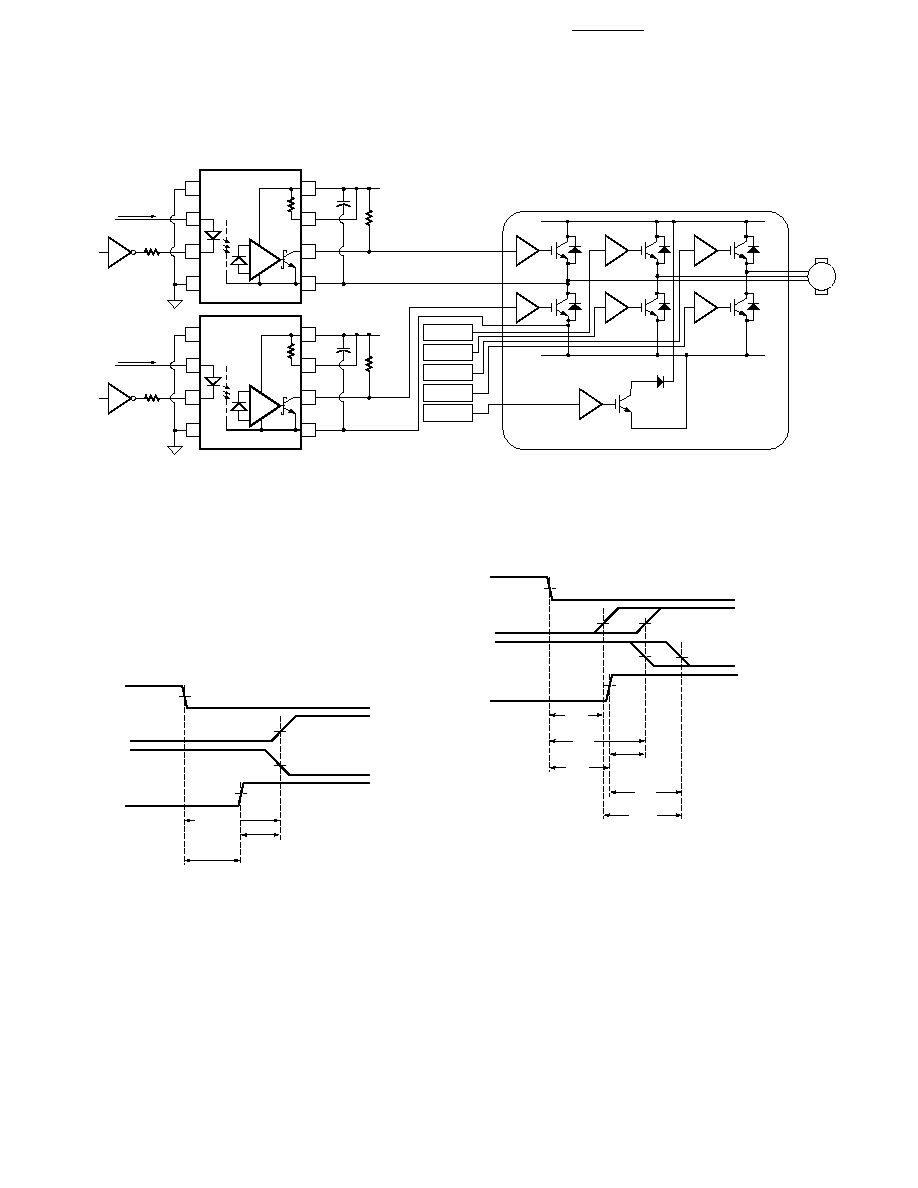
Figure 24. Typical Application Circuit.
Figure 26. Waveforms for Dead Time Calculation.
Figure 25. Minimum LED Skew for Zero Dead Time.
0.1 µF
20 k
CMOS
310
+5 V
V
OUT1
I
LED1
V
CC1
M
HCPL-4506
HCPL-4506
HCPL-4506
HCPL-4506
HCPL-4506
Q2
Q1
-HV
+HV
IPM
8
7
6
1
3
SHIELD
5
2
4
20 k
HCPL-4506
0.1 µF
20 k
CMOS
310
+5 V
V
OUT2
I
LED2
V
CC2
8
7
6
1
3
SHIELD
5
2
4
20 k
HCPL-4506
VOUT1
VOUT2
ILED2
tPLH MAX.
PDD* MAX. =
(tPLH-tPHL) MAX. = tPLH MAX. - tPHL MIN.
tPHL
MIN.
ILED1
Q1 ON
Q2 OFF
Q1 OFF
Q2 ON
*PDD = PROPAGATION DELAY DIFFERENCE
NOTE: THE PROPAGATION DELAYS USED TO CALCULATE
PDD ARE TAKEN AT EQUAL TEMPERATURES.
VOUT1
VOUT2
ILED2
tPLH
MIN.
MAXIMUM DEAD TIME
(DUE TO OPTOCOUPLER)
= (t
PLH MAX.
- t
PLH MIN.
) + (t
PHL MAX.
- t
PHL MIN.
)
= (t
PLH MAX.
- t
PHL MIN.
) - (t
PLH MIN.
- t
PHL MAX.
)
= PDD* MAX. - PDD* MIN.
tPHL
MIN.
ILED1
Q1 ON
Q2 OFF
Q1 OFF
Q2 ON
*PDD = PROPAGATION DELAY DIFFERENCE
tPLH
MAX.
tPHL
MAX.
PDD*
MAX.
MAX.
DEAD TIME
NOTE: THE PROPAGATION DELAYS USED TO CALCULATE THE MAXIMUM
DEAD TIME ARE TAKEN AT EQUAL TEMPERATURES.

17
LED Drive Circuit
Considerations for Ultra
High CMR Performance
Without a detector shield, the
dominant cause of optocoupler
CMR failure is capacitive coupl-
ing from the input side of the
optocoupler, through the
package, to the detector IC
as shown in Figure 16. The
HCPL-4506 series improve
CMR performance by using a
detector IC with an optically
transparent Faraday shield, which
diverts the capacitively coupled
current away from the sensitive
IC circuitry. However, this shield
does not eliminate the capacitive
coupling between the LED and
the optocoupler output pins and
output ground as shown in Figure
17. This capacitive coupling
causes perturbations in the LED
current during common mode
transients and becomes the
major source of CMR failures
for a shielded optocoupler. The
main design objective of a high
CMR LED drive circuit becomes
keeping the LED in the proper
state (on or off) during common
mode transients. For example,
the recommended application
circuit (Figure 15), can achieve
15 kV/
µ
s CMR while minimizing
component complexity. Note that
a CMOS gate is recommended
in Figure 15 to keep the LED
off when the gate is in the high
state.
Another cause of CMR failure for
a shielded optocoupler is direct
coupling to the optocoupler
output pins through C
LEDO1
and
C
LEDO2
in Figure 17. Many factors
influence the effect and magni-
tude of the direct coupling
including: the use of an internal
or external output pull-up
resistor, the position of the LED
current setting resistor, the
connection of the unused input
package pins, and the value of the
capacitor at the optocoupler
output (C
L
).
Techniques to keep the LED in
the proper state and minimize the
effect of the direct coupling are
discussed in the next two
sections.
CMR with the LED On
(CMR
L
)
A high CMR LED drive circuit
must keep the LED on during
common mode transients. This is
achieved by overdriving the LED
current beyond the input
threshold so that it is not pulled
below the threshold during a
transient. The recommended
minimum LED current of 10 mA
provides adequate margin over
the maximum I
TH
of 5.0 mA (see
Figure 1) to achieve 15 kV/
µ
s
CMR. Capacitive coupling is
higher when the internal load
resistor is used (due to C
LEDO2
)
and an I
F
= 16 mA is required to
obtain 10 kV/
µ
s CMR.
The placement of the LED current
setting resistor effects the ability
of the drive circuit to keep the
LED on during transients and
interacts with the direct coupling
to the optocoupler output. For
example, the LED resistor in
Figure 18 is connected to the
anode. Figure 19 shows the AC
equivalent circuit for Figure 18
during common mode transients.
During a +dVcm/dt in Figure 19,
the current available at the LED
anode (Itotal) is limited by the
series resistor. The LED current
(I
F
) is reduced from its DC value
by an amount equal to the current
that flows through C
LEDP
and
C
LEDO1
. The situation is made
worse because the current
through C
LEDO1
has the effect of
trying to pull the output high
(toward a CMR failure) at the
same time the LED current is
being reduced. For this reason,
the recommended LED drive
circuit (Figure 15) places the
current setting resistor in series
with the LED cathode. Figure 20
is the AC equivalent circuit for
Figure 15 during common mode
transients. In this case, the LED
current is not reduced during a
+dVcm/dt transient because the
current flowing through the
package capacitance is supplied
by the power supply. During a
-dVcm/dt transient, however, the
LED current is reduced by the
amount of current flowing
through C
LEDN
. But, better CMR
performance is achieved since the
current flowing in C
LEDO1
during a
negative transient acts to keep the
output low.
Coupling to the LED and output
pins is also affected by the con-
nection of pins 1 and 4. If CMR is
limited by perturbations in the
LED on current, as it is for the
recommended drive circuit
(Figure 15), pins 1 and 4 should
be connected to the input circuit
common. However, if CMR
performance is limited by direct
coupling to the output when the
LED is off, pins 1 and 4 should be
left unconnected.
CMR with the LED Off
(CMR
H
)
A high CMR LED drive circuit
must keep the LED off
(V
F
V
F(OFF)
) during common
mode transients. For example,
during a +dVcm/dt transient in
Figure 20, the current flowing
through C
LEDN
is supplied by the
parallel combination of the LED
and series resistor. As long as the
voltage developed across the
resistor is less than V
F(OFF)
the

18
LED will remain off and no
common mode failure will occur.
Even if the LED momentarily
turns on, the 100 pF capacitor
from pins 6-5 will keep the output
from dipping below the threshold.
The recommended LED drive
circuit (Figure 15) provides about
10 V of margin between the
lowest optocoupler output voltage
and a 3 V IPM threshold during
a 15 kV/
µ
s transient with
V
CM
= 1500 V. Additional margin
can be obtained by adding a diode
in parallel with the resistor, as
shown by the dashed line con-
nection in Figure 20, to clamp
the voltage across the LED
below V
F(OFF)
.
Since the open collector drive
circuit, shown in Figure 21,
cannot keep the LED off during
a +dVcm/dt transient, it is
not desirable for applications
requiring ultra high CMR
H
performance. Figure 22 is the AC
equivalent circuit for Figure 21
during common mode transients.
Essentially all the current flowing
through C
LEDN
during a +dVcm/dt
transient must be supplied by
the LED. CMR
H
failures can occur
at dV/dt rates where the current
through the LED and C
LEDN
exceeds the input threshold.
Figure 23 is an alternative drive
circuit which does achieve ultra
high CMR performance by
shunting the LED in the off state.
IPM Dead Time and
Propagation Delay
Specifications
The HCPL-4506 series include
a Propagation Delay Difference
specification intended to help
designers minimize "dead time"
in their power inverter designs.
Dead time is the time period
during which both the high and
low side power transistors (Q1
and Q2 in Figure 24) are off. Any
overlap in Q1 and Q2 conduction
will result in large currents flow-
ing through the power devices
between the high and low voltage
motor rails.
To minimize dead time the
designer must consider the propa-
gation delay characteristics of the
optocoupler as well as the charac-
teristics of the IPM IGBT gate
drive circuit. Considering only the
delay characteristics of the opto-
coupler (the characteristics of the
IPM IGBT gate drive circuit can
be analyzed in the same way) it is
important to know the minimum
and maximum turn-on (t
PHL
) and
turn-off (t
PLH
) propagation delay
specifications, preferably over the
desired operating temperature
range.
The limiting case of zero dead
time occurs when the input to Q1
turns off at the same time that the
input to Q2 turns on. This case
determines the minimum delay
between LED1 turn-off and LED2
turn-on, which is related to the
worst case optocoupler propaga-
tion delay waveforms, as shown in
Figure 25. A minimum dead time
of zero is achieved in Figure 25
when the signal to turn on LED2
is delayed by (t
PLH max
- t
PHL min
)
from the LED1 turn off. Note that
the propagation delays used to
calculate PDD are taken at equal
temperatures since the opto-
couplers under consideration
are typically mounted in close
proximity to each other.
(Specifically, t
PLH max
and t
PHL min
in the previous equation are not
the same as the t
PLH max
and
t
PHL min
, over the full operating
temperature range, specified in
the data sheet.) This delay is the
maximum value for the propaga-
tion delay difference specification
which is specified at 450 ns for
the HCPL-4506 series over an
operating temperature range of
-40
∞
C to 100
∞
C.
Delaying the LED signal by the
maximum propagation delay dif-
ference ensures that the minimum
dead time is zero, but it does not
tell a designer what the maximum
dead time will be. The maximum
dead time occurs in the highly
unlikely case where one opto-
coupler with the fastest t
PLH
and
another with the slowest t
PHL
are in the same inverter leg. The
maximum dead time in this case
becomes the sum of the spread
in the t
PLH
and t
PHL
propagation
delays as shown in Figure 26.
The maximum dead time is also
equivalent to the difference
between the maximum and mini-
mum propagation delay difference
specifications. The maximum
dead time (due to the optocoup-
lers) for the HCPL-4506 series
is 600 ns (= 450 ns - (-150 ns) )
over an operating temperature
range of -40
∞
C to 100
∞
C.

19

www.semiconductor.agilent.com
Data subject to change.
Copyright © 2001 Agilent Technologies, Inc.
September 6, 2001
Obsoletes 5968-1089E (11/99)
5988-4107EN