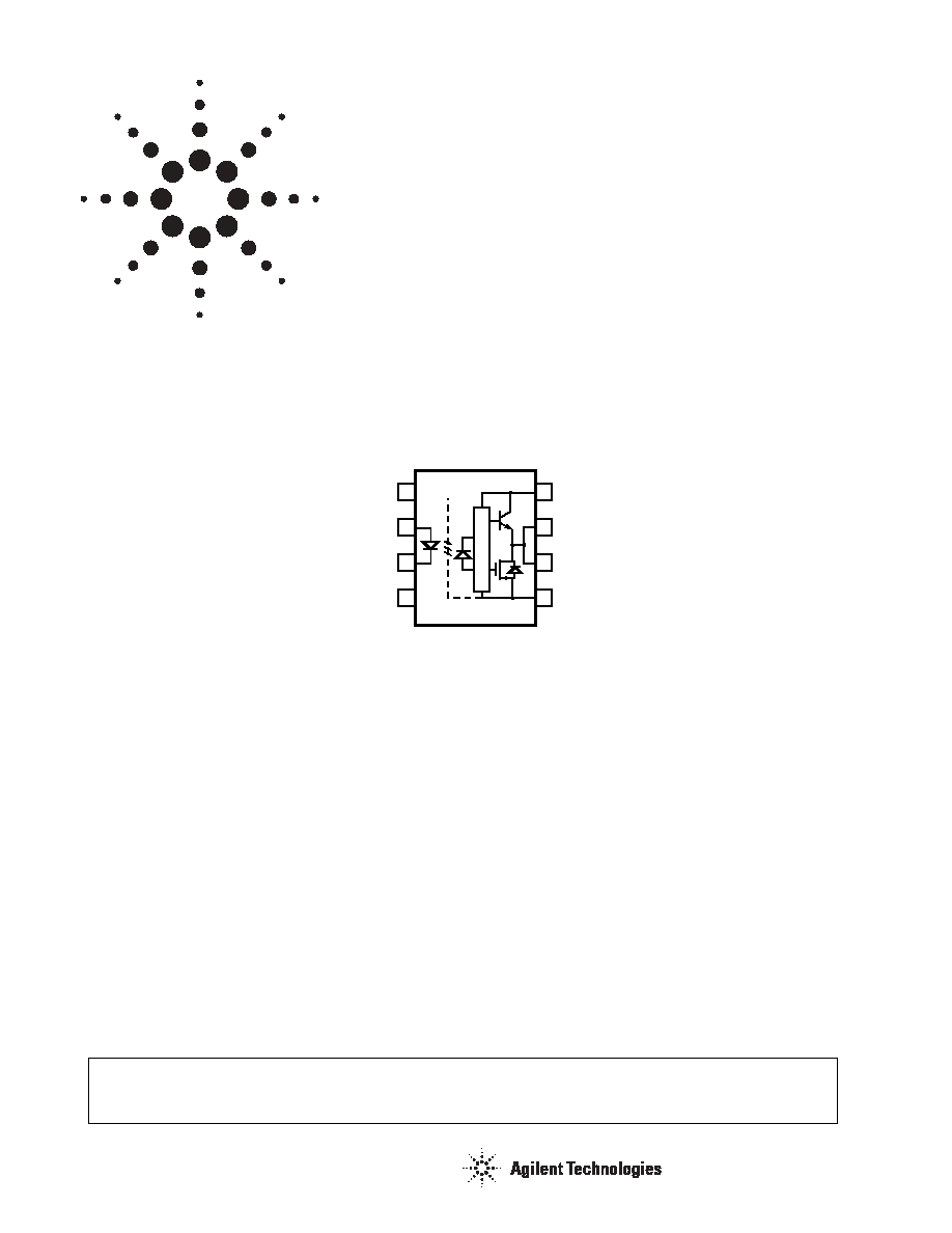
Description
The HCPL- 5150 contains a
GaAsP LED optically coupled to
an integrated circuit with a
power output stage. The device
is ideally suited for driving
power IGBTs and MOSFETs
used in motor control inverter
applications. The high
operating voltage range of the
output stage provides the drive
voltages required by gate
controlled devices. The voltage
and current supplied by this
optocoupler makes it ideally
suited for directly driving IGBTs
with ratings up to 1200 V/50 A.
For IGBTs with higher ratings,
the HCPL- 5150 can be used to
drive a discrete power stage,
which drives the IGBT gate.
The products are capable of
operation and storage over the
full military temperature range
and can be purchased as either
commercial product, with full
MIL- PRF- 38534 Class H testing,
or from Defense Supply Center
Columbus (DSCC) Standard
Microcircuit Drawing (SMD)
5962- 04205. All devices are
manufactured and tested on a
Agilent HCPL-5150 & HCPL-5151
DSCC SMD 5962-04205
0.5 Amp Output Current IGBT
Gate Drive Optocoupler
Data Sheet
MIL- PRF- 38534 certified line
and are included in the DSCC
Qualified Manufacturers List,
QML- 38534 for Hybrid
Microcircuits.
Schematic Diagram
Applications
∑ Industrial and Military
Environments
∑ High Reliability Systems
∑ Harsh Industrial Environments
∑ Transportation, Medical, and Life
Critical Systems
∑ Isolated IGBT/MOSFET Gate Drive
∑ AC and Brushless DC Motor Drives
∑ Industrial Inverters
∑ Switch Mode Power Supplies
(SMPS)
∑ Uninterruptible Power Supplies
(UPS)
1
3
SHIELD
2
4
8
6
7
5
N/C
CATHODE
ANODE
N/C
VCC
VO
VO
VEE
Features
∑
Performance Guaranteed over Full
Military Temperature Range:
-55
∞
C to +125
∞
C
∑ Manufactured and Tested on a MIL-
PRF-38534 Certified Line
∑ Hermetically Sealed Packages
∑ Dual Marked with Device Part
Number and DSCC Drawing
Number
∑ QML-38534
∑ HCPL-3150 Function Compatibility
∑ 0.5 A Minimum Peak Output Current
∑
10 kV/
µ
s Minimum Common Mode
Rejection (CMR) at V
CM
= 1000 V
∑ 1.0 V Maximum Low Level Output
Voltage (V
OL
) Eliminates Need for
Negative Gate Drive
∑ I
CC
= 5 mA Maximum Supply
Current
∑ Under Voltage Lock-Out Protection
(UVLO) with Hysteresis
∑ Wide Operating V
CC
Range: 15 to 30
Volts
∑ 500 ns Maximum Propagation Delay
∑
+/- 0.35
µ
s Maximum Delay
Between Devices
CAUTION: It is advised that normal static precautions be taken in handling and assembly of
this component to prevent damage and/or degradation which may be induced by ESD.
2
Truth Table
A 0.1
µ
F bypass capacitor must be connected between pins 5 and 8.
Device Marking
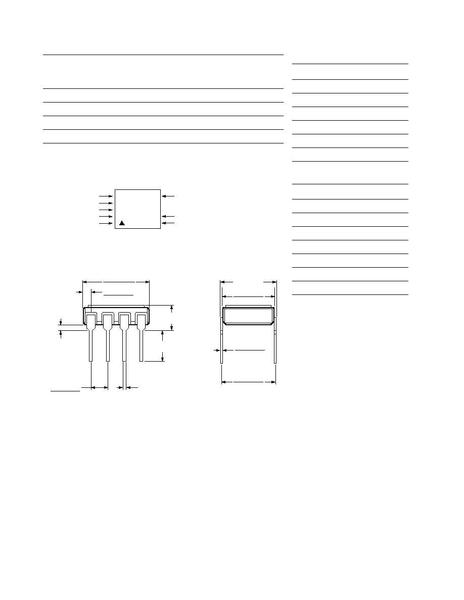
Outline Drawing
LED
V
CC
-
V
EE
"POSITIVE GOING"
(i.e., TURN-ON)
V
CC
-
V
EE
"NEGATIVE GOING"
(i.e., TURN-OFF)
V
O
OFF
0
-
30 V
0
-
30 V
LOW
ON
0
-
11 V
0
-
9.5 V
LOW
ON
11
-
13.5 V
9.5
-
12 V
TRANSITION
ON
13.5
-
30 V
12
-
30 V
HIGH
COMPLIANCE INDICATOR,*
DATE CODE, SUFFIX (IF NEEDED)
A
HCPL-515x
5962-04205
01Hxx
50434
COUNTRY OF MFR.
Agilent CAGE CODE*
Agilent DESIGNATOR
DSCC SMD*
PIN ONE/
ESD IDENT
Agilent P/N
DSCC SMD*
* QUALIFIED PARTS ONLY
SGP
QYYWWZ
3.81 (0.150)
MIN.
4.32 (0.170)
MAX.
9.40 (0.370)
9.91 (0.390)
0.51 (0.020)
MAX.
2.29 (0.090)
2.79 (0.110)
0.51 (0.020)
MIN.
0.76 (0.030)
1.27 (0.050)
8.13 (0.320)
MAX.
7.36 (0.290)
7.87 (0.310)
0.20 (0.008)
0.33 (0.013)
7.16 (0.282)
7.57 (0.298)
NOTE: DIMENSIONS IN MILLIMETERS (INCHES).
Selection Guide
-
Package Styles and
Lead Configuration Options
Agilent Part Number and Options
Commercial
HCPL-5150
MIL-PRF-38534, Class H HCPL-5151
Standard Lead Finish
Gold Plate
Solder Dipped
Option
-
200
Butt Cut/Gold Plate
Option
-
100
Gull Wing/Soldered
Option
-
300
SMD Part Number
Prescript for all below
5962-
Either Gold or Solder
0420501HPX
Gold Plate
0420501HPC
Solder Dipped
0420501HPA
Butt Cut/Gold Plate
0420501HYC
Butt Cut/Soldered
0420501HYA
Gull Wing/Soldered
0420501HXA
3
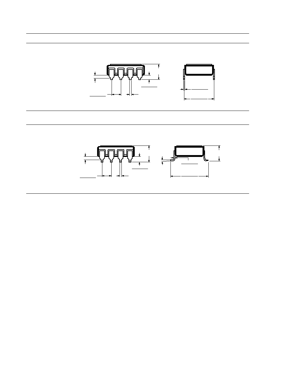
Hermetic Optocoupler Options
Option
Description
100
Surface mountable hermetic optocoupler with leads trimmed for butt joint assembly. This option is available
on commercial and hi-rel product (see drawings below for details).
200
Lead finish is solder dipped rather than gold plated. This option is available on commercial and hi-rel product.
DSCC Drawing part numbers contain provisions for lead finish.
300
Surface mountable hermetic optocoupler with leads cut and bent for gull wing assembly. This option is avail-
able on commercial and hi-rel product (see drawings below for details). This option has solder dipped leads.
1.14 (0.045)
1.40 (0.055)
4.32 (0.170)
MAX.
0.51 (0.020)
MAX.
2.29 (0.090)
2.79 (0.110)
0.51 (0.020)
MIN.
7.36 (0.290)
7.87 (0.310)
0.20 (0.008)
0.33 (0.013)
NOTE: DIMENSIONS IN MILLIMETERS (INCHES).
0.51 (0.020)
MIN.
4.57 (0.180)
MAX.
0.51 (0.020)
MAX.
2.29 (0.090)
2.79 (0.110)
1.40 (0.055)
1.65 (0.065)
9.65 (0.380)
9.91 (0.390)
5
o
MAX.
4.57 (0.180)
MAX.
0.20 (0.008)
0.33 (0.013)
NOTE: DIMENSIONS IN MILLIMETERS (INCHES).
4
Absolute Maximum Ratings
Notes:
1. No derating required with the typical case-to-ambient thermal resistance. (
CA
=140
∞
C/W) Refer to Figure 35.
2. Maximum pulse width = 10
µ
s, maximum duty cycle = 0.2%. This value is intended to allow for component tolerances for designs with I
O
peak minimum
= 0.5 A. See Applications section for additional details on limiting I
OH
peak.
3. Derate linearly above 102
∞
C free air temperature at a rate of 6mW/
∞
C with the typical case-to-ambient thermal resistance (
CA
=140
∞
C/W).
Refer to Figure 36.
4. Derate linearly above 102
∞
C free air temperature at a rate of 6mW/
∞
C with the typical case-to-ambient thermal resistance (
CA
=140
∞
C/W).
Refer to Figure 35 and 36.
ESD Classification
Recommended Operating Conditions
Parameter
Symbol
Min.
Max.
Units
Note
Storage Temperature
T
S
-65
+150
∞
C
Operating Temperature
T
A
-55
+125
∞
C
Case Temperature
T
C
+145
∞
C
Junction Temperature
T
J
+150
∞
C
Lead Solder Temperature
260 for 10s
∞
C
Average Input Current
I
F
AVG
25
mA
1
Peak Transient Input Current
(<1
µ
s pulse width, 300 pps)
I
F
PK
1.0
A
Reverse Input Voltage
V
R
5
V
"High" Peak Output Current
I
OH (PEAK)
0.6
A
2
"Low" Peak Output Current
I
OL (PEAK)
0.6
A
2
Supply Voltage
(V
CC
-V
EE
)
0
35
V
Output Voltage
V
O
(PEAK)
0
V
CC
V
Input Power Dissipation
P
E
45
mW
1
Output Power Dissipation
P
O
250
mW
3
Total Power Dissipation
P
T
295
mW
4
MIL-STD-883, Method 3015
(
), Class 1
Parameter
Symbol
Min.
Max.
Units
Power Supply Voltage
(V
CC
≠ V
EE
)
15
30
Volts
Input Current (ON)
I
F
(ON)
10
18
mA
Input Voltage (OFF)
V
F
(OFF)
-3.0
0.8
Volts
Operating Temperature
T
A
-55
125
∞
C
5
Electrical Specifications (DC)
Over recommended operating conditions (T
A
= -55 to +125
∞
C, I
F(ON)
= 10 to 18 mA, V
F(OFF)
= -3.0 to 0.8V, V
CC
= 15 to 30 V,
V
EE
= Ground) unless otherwise specified.
Parameter
Symbol
Test Conditions
Group A
Subgroups
(13)
Limits
Units
Fig.
Note
Min.
Typ.*
Max.
High Level
Output Current
I
OH
V
O
=
(V
CC
-
4 V)
1, 2, 3
0.1
0.4
A
2, 3, 17
2
V
O
=
(V
CC
-
15 V)
0.5
1
Low Level
Output Current
I
OL
V
O
= (V
EE
+ 2.5 V)
1, 2, 3
0.1
0.6
A
5, 6, 18
2
V
O
= (V
EE
+ 15 V)
0.5
1
High Level
Output Voltage
V
OH
I
O
= -100 mA
1, 2, 3
(V
CC
-
4) (V
CC
-
3)
V
1, 3, 19
3, 4
Low Level
Output Voltage
V
OL
I
O
= 100 mA
1, 2, 3
0.4
1.0
V
4, 6, 20
High Level
Supply Current
I
CCH
Output Open,
I
F
= 10 to 18 mA
1, 2, 3
2.5
5.0
mA
7, 8
Low Level
Supply Current
I
CCL
Output Open,
V
F
= -3.0 to +0.8V
1, 2, 3
2.7
5.0
mA
Threshold Input Cur-
rent Low to High
I
FLH
I
O
= 0 mA,
V
O
> 5 V
1, 2, 3
2.6
9.0
mA
9, 15,
21
Threshold Input
Voltage High to Low
V
FHL
1, 2, 3
0.8
V
Input Forward
Voltage
V
F
I
F
= 10 mA
1, 2, 3
1.2
1.5
1.8
V
16
Temperature
Coefficient of
Forward Voltage
V
F
/
T
A
I
F
= 10 mA
-1.6
mV/
∞
C
Input Reverse
Breakdown Voltage
BV
R
I
R
= 10
µ
A
1, 2, 3
5
V
Input Capacitance
C
IN
f = 1 MHz,
V
F
= 0 V
80
pF
UVLO Threshold
V
UVLO+
V
O
> 5 V,
I
F
= 10 mA
1, 2, 3
11.0
12.3
13.5
V
22, 37
V
UVLO-
1, 2, 3
9.5
10.7
12.0
UVLO Hysteresis
UVLO
HYS
1.6
*All typical values at T
A
= 25
∞
C and V
CC
-
V
EE
= 30 V, unless otherwise noted.