Hermetically Sealed,
Low I
F
, Wide V
CC
,
Logic Gate Optocouplers
Technical Data
Features
∑ Dual Marked with Device
Part Number and DSCC
Standard Microcircuit
Drawing
∑ Manufactured and Tested on
a MIL-PRF-38534 Certified
Line
∑ QML-38534, Class H and K
∑ Four Hermetically Sealed
Package Configurations
∑ Performance Guaranteed
over -55
∞
C to +125
∞
C
∑ Wide V
CC
Range (4.5 to 20 V)
∑ 350 ns Maximum Propaga-
tion Delay
∑ CMR: > 10,000 V/
µ
s Typical
∑ 1500 Vdc Withstand Test
Voltage
∑ Three State Output Available
∑ High Radiation Immunity
∑ HCPL-2200/31 Function
Compatibility
∑ Reliability Data Available
∑ Compatible with LSTTL,
TTL, and CMOS Logic
Applications
∑ Military and Space
∑ High Reliability Systems
∑ Transportation and Life
Critical Systems
∑ High Speed Line Receiver
CAUTION: It is advised that normal static precautions be taken in handling and assembly of this component to
prevent damage and/or degradation which may be induced by ESD.
∑ Isolated Bus Driver (Single
Channel)
∑ Pulse Transformer
Replacement
∑ Ground Loop Elimination
∑ Harsh Industrial
Environments
∑ Computer-Peripheral
Interfaces
Description
These units are single, dual and
quad channel, hermetically sealed
optocouplers. The products are
capable of operation and storage
over the full military temperature
range and can be purchased as
either standard product or with
full MIL-PRF-38534 Class Level
H or K testing or from the
appropriate DSCC Drawing. All
devices are manufactured and
tested on a MIL-PRF-38534
certified line and are included in
the DSCC Qualified Manufac-
turers List QML-38534 for Hybrid
Microcircuits.
Each channel contains an AlGaAs
light emitting diode which is
optically coupled to an integrated
high gain photon detector. The
detector has a threshold with
hysteresis which provides differ-
ential mode noise immunity and
eliminates the potential for
output signal chatter. The
detector in the single channel
units has a tri-state output stage
Truth Tables
(Positive Logic)
Multichannel Devices
Input
Output
On (H)
H
Off (L)
L
HCPL-520x*
5962-88768
HCPL-523x
HCPL-623x
HCPL-625x
5962-88769
*See matrix for available extensions.
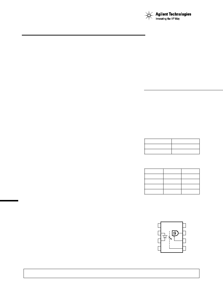
Functional Diagram
Multiple Channel Devices
Available
VCC
VO
VE
GND
Single Channel DIP
Input
Enable
Output
On (H)
H
Z
Off (L)
H
Z
On (H)
L
H
Off (L)
L
L
A 0.1
µ
F bypass capacitor must be connected between V
CC
and GND pins.

2
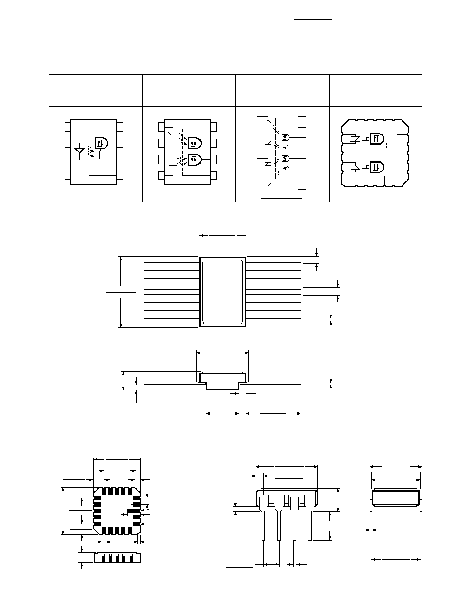
Selection Guide≠Package Styles and Lead Configuration Options
Package
8 Pin DIP
8 Pin DIP
16 Pin Flat Pack
20 Pad LCCC
Lead Style
Through Hole
Through Hole
Unformed Leads
Surface Mount
Channels
1
2
4
2
Common Channel
None
V
CC
, GND
V
CC
, GND
None
Wiring
Agilent Part # & Options
Commercial
HCPL-5200
HCPL-5230
HCPL-6250
HCPL-6230
MIL-PRF-38534, Class H
HCPL-5201
HCPL-5231
HCPL-6251
HCPL-6231
MIL-PRF-38534, Class K
HCPL-520K
HCPL-523K
HCPL-625K
HCPL-623K
Standard Lead Finish
Gold Plate
Gold Plate
Gold Plate
Soldered Pads
Solder Dipped
Option #200
Option #200
Butt Cut/Gold Plate
Option #100
Option #100
Gull Wing/Soldered
Option #300
Option #300
Class H SMD Part #
Prescript for all below
5962-
5962-
5962-
5962-
Either Gold or Solder
8876801PX
8876901PX
8876903FX
88769022X
Gold Plate
8876801PC
8876901PC
8876903FC
Solder Dipped
8876801PA
8876901PA
88769022A
Butt Cut/Gold Plate
8876801YC
8876901YC
Butt Cut/Soldered
8876801YA
8876901YA
Gull Wing/Soldered
8876801XA
8876901XA
Class K SMD Part #
Prescript for all below
5962-
5962-
5962-
5962-
Either Gold or Solder
8876802KPX
8876904KPX
8876906KFX
8876905K2X
Gold Plate
8876802KPC
8876904KPC
8876906KFC
Solder Dipped
8876802KPA
8876904KPA
8876905K2A
Butt Cut/Gold Plate
8876802KYC
8876904KYC
Butt Cut/Soldered
8876802KYA
8876904KYA
Gull Wing/Soldered
8876802KXA
8876904KXA
which allows for direct connection
to data buses. The output is non-
inverting. The detector IC has an
internal shield that provides a
guaranteed common mode
transient immunity of up to
10,000 V/
µ
s. Improved power
supply rejection eliminates the
need for special power supply
bypass precautions.
Package styles for these parts are
8 pin DIP through hole (case
outline P), 16 pin DIP flat pack
(case outline F), and leadless
ceramic chip carrier (case outline
2). Devices may be purchased
with a variety of lead bend and
plating options, see Selection
Guide Table for details. Standard
Microcircuit Drawing (SMD)
parts are available for each
package and lead style.
Because the same electrical die
(emitters and detectors) are used
for each channel of each device
listed in this data sheet, absolute
maximum ratings, recommended
operating conditions, electrical
specifications, and performance
characteristics shown in the
figures are identical for all parts.
Occasional exceptions exist due
to package variations and limita-
tions and are as noted. Addition-
ally, the same package assembly
processes and materials are used
in all devices. These similarities
give justification for the use of
data obtained from one part to
represent other part's per-
formance for die related
reliability and certain limited
radiation test results.
3
Functional Diagrams
8 Pin DIP
8 Pin DIP
16 Pin Flat Pack
20 Pad LCCC
Through Hole
Through Hole
Unformed Leads
Surface Mount
1 Channel
2 Channels
4 Channels
2 Channels
Note: Multichannel DIP and flat pack devices have common V
CC
and ground. Single channel DIP has an enable pin 6. LCCC (leadless
ceramic chip carrier) package has isolated channels with separate V
CC
and ground connections.
VCC
7
5
6
8
VO
VE
GND
1
2
3
4
Outline Drawings
16 Pin Flat Pack, 4 Channels
VCC
7
5
6
8
VO1
GND
1
2
3
4
VO2
8 Pin DIP Through Hole, 1 and 2 Channel
20 Terminal LCCC Surface Mount, 2 Channels
5
7
6
8
12
10
11
9
GND
VO4
VO3
1
3
2
4
16
14
15
13
VCC
VO2
VO1
GND1
VO2
19
20
2
3
VO1
8
7
VCC2
VCC1
10
GND2
15
13
12
8.13 (0.320)
MAX.
5.23
(0.206)
MAX.
2.29 (0.090)
MAX.
7.24 (0.285)
6.99 (0.275)
1.27 (0.050)
REF.
0.46 (0.018)
0.36 (0.014)
11.13 (0.438)
10.72 (0.422)
2.85 (0.112)
MAX.
0.89 (0.035)
0.69 (0.027)
0.31 (0.012)
0.23 (0.009)
0.88 (0.0345)
MIN.
9.02 (0.355)
8.76 (0.345)
NOTE: DIMENSIONS IN MILLIMETERS (INCHES).
8.70 (0.342)
9.10 (0.358)
4.95 (0.195)
5.21 (0.205)
1.78 (0.070)
2.03 (0.080)
1.02 (0.040) (3 PLCS)
4.95 (0.195)
5.21 (0.205)
8.70 (0.342)
9.10 (0.358)
1.78 (0.070)
2.03 (0.080)
0.51 (0.020)
0.64
(0.025)
(20 PLCS)
1.52 (0.060)
2.03 (0.080)
METALIZED
CASTILLATIONS (20 PLCS)
2.16 (0.085)
TERMINAL 1 IDENTIFIER
NOTE: DIMENSIONS IN MILLIMETERS (INCHES).
SOLDER THICKNESS 0.127 (0.005) MAX.
1.14 (0.045)
1.40 (0.055)
3.81 (0.150)
MIN.
4.32 (0.170)
MAX.
9.40 (0.370)
9.91 (0.390)
0.51 (0.020)
MAX.
2.29 (0.090)
2.79 (0.110)
0.51 (0.020)
MIN.
0.76 (0.030)
1.27 (0.050)
8.13 (0.320)
MAX.
7.36 (0.290)
7.87 (0.310)
0.20 (0.008)
0.33 (0.013)
7.16 (0.282)
7.57 (0.298)
NOTE: DIMENSIONS IN MILLIMETERS (INCHES).
4
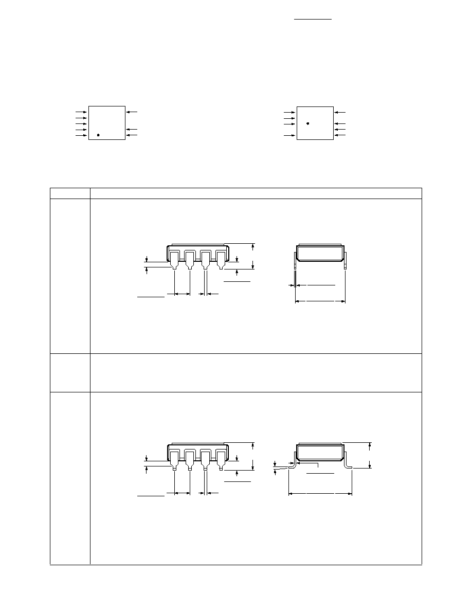
Hermetic Optocoupler Options
Option
Description
100
Surface mountable hermetic optocoupler with leads trimmed for butt joint assembly. This
option is available on commercial and hi-rel product in 8 pin DIP (see drawings below for
details).
200
Lead finish is solder dipped rather than gold plated. This option is available on commercial
and hi-rel product in 8 pin DIP. DSCC Drawing part numbers contain provisions for lead
finish. All leadless chip carrier devices are delivered with solder dipped terminals as a
standard feature.
300
Surface mountable hermetic optocoupler with leads cut and bent for gull wing assembly. This
option is available on commercial and hi-rel product in 8 pin DIP (see drawings below for
details). This option has solder dipped leads.
Leadless Device Marking
Leaded Device Marking
*QUALIFIED PARTS ONLY
*QUALIFIED PARTS ONLY
1.14 (0.045)
1.40 (0.055)
4.32 (0.170)
MAX.
0.51 (0.020)
MAX.
2.29 (0.090)
2.79 (0.110)
0.51 (0.020)
MIN.
7.36 (0.290)
7.87 (0.310)
0.20 (0.008)
0.33 (0.013)
NOTE: DIMENSIONS IN MILLIMETERS (INCHES).
0.20 (0.008)
0.33 (0.013)
0.51 (0.020)
MIN.
4.57 (0.180)
MAX.
0.51 (0.020)
MAX.
2.29 (0.090)
2.79 (0.110)
1.40 (0.055)
1.65 (0.065)
9.65 (0.380)
9.91 (0.390)
5∞ MAX.
4.57 (0.180)
MAX.
NOTE: DIMENSIONS IN MILLIMETERS (INCHES).
COMPLIANCE INDICATOR,*
DATE CODE, SUFFIX (IF NEEDED)
A QYYWWZ
XXXXXX
XXXXXXX
XXX XXX
50434
COUNTRY OF MFR.
Agilent FSCN*
Agilent LOGO
DSCC SMD*
PIN ONE/
ESD IDENT
Agilent P/N
DSCC SMD*
COMPLIANCE INDICATOR,*
DATE CODE, SUFFIX (IF NEEDED)
A QYYWWZ
XXXXXX
XXXX
XXXXXX
XXX 50434
DSCC SMD*
Agilent FSCN*
Agilent LOGO
COUNTRY OF MFR.
Agilent P/N
PIN ONE/
ESD IDENT
DSCC SMD*
5
Absolute Maximum Ratings
Storage Temperature Range, T
S
.................................. -65
∞
C to +150
∞
C
Operating Temperature, T
A
......................................... -55
∞
C to +125
∞
C
Case Temperature, T
C
................................................................ +170
∞
C
Junction Temperature, T
J
.......................................................... +175
∞
C
Lead Solder Temperature .............................................. 260
∞
C for 10 s
Average Forward Curre, I
F AVG
(each channel) ............................. 8 mA
Peak Input Current, I
F PK
(each channel) ............................... 20 mA
[1]
Reverse Input Voltage, V
R
(each channel) ....................................... 3 V
Supply Voltage ,V
CC
.............................................. 0.0 V min., 20 V max.
Average Output Current, I
O
(each channel) ................................. 15 mA
Output Voltage, V
O
(each channel) .................... ≠0.3 V min., 20 V max.
Package Power Dissipation, P
d
(each channel) ......................... 200 mW
Single Channel Product Only
Tri-State Enable Voltage, V
E
............................... ≠0.3 V min., 20 V max.
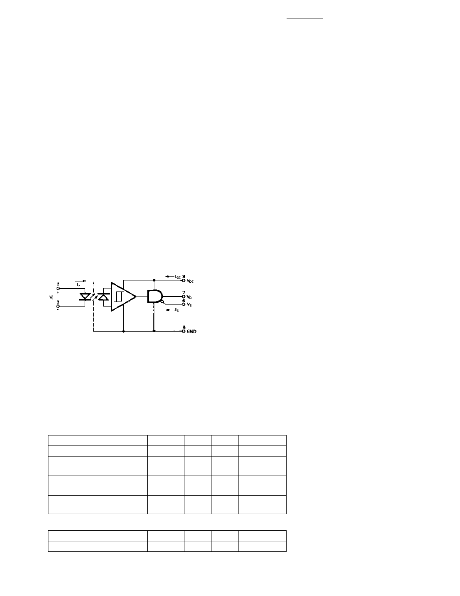
8 Pin Ceramic DIP Single Channel Schematic
Recommended Operating Conditions
Parameter
Symbol
Min.
Max.
Units
Power Supply Voltage
V
CC
4.5
20
V
Input Current, High Level,
I
FH
2
8
mA
Each Channel
Input Voltage, Low Level,
V
FL
0
0.8
V
Each Channel
Fan Out (TTL Load)
N
4
Each Channel
Single Channel Product Only
High Level Enable Voltage
V
EH
2.0
20
V
Low Level Enable Voltage
V
EL
0
0.8
V
Note enable pin 6. An external 0.01
µ
F to 0.1
µ
F bypass capacitor is recommended
between V
CC
and ground for each package type.
ESD Classification
(MIL-STD-883, Method 3015)
HCPL-5200/01/0K, HCPL-6230/31/3K ................................ (
), Class 1
HCPL-5230/31/3K, HCPL-6250/51/5K ............................ (Dot), Class 3
ANODE
CATHODE
6
Electrical Characteristics
T
A
= -55
∞
C to +125
∞
C, 4.5 V
V
CC
20 V, 2 mA
I
F(ON)
8 mA, 0 V
V
F(OFF)
0.8 V, unless otherwise
specified.
Group A
[11]
Limit
Parameter
Sym. Test
Conditions
Subgroups
Min. Typ.* Max. Units Fig. Notes
Logic Low Output Voltage
V
OL
I
OL
= 6.4 mA (4 TTL Loads)
1, 2, 3
0.5
V
1, 3
2
I
OH
= -2.6 mA
1, 2, 3
2.4
**
V
Logic High Output Voltage
V
OH
(**V
OH
= V
CC
- 2.1 V)
2, 3
2
I
OH
= -0.32 mA
NA
3.1
Output Leakage Current
I
OHH
V
O
= 5.5 V
I
F
= 8 mA
1, 2, 3
100
µ
A
2
(V
OUT
> V
CC
)
V
O
= 20 V
V
CC
= 4.5 V
500
Single
V
CC
= 5.5 V V
F
= 0 V
4.5
6
Channel
V
E
= Don't Care
Logic Low
V
CC
= 20 V
1, 2, 3
5.3
7.5
Supply
I
CCL
Current
Dual
V
CC
= 5.5 V
9.0
12
mA
Channel
V
F1
= V
F2
= 0 V
V
CC
= 20 V
10.6
15
Quad
V
CC
= 5.5 V V
F1
= V
F2
=
14
24
Channel
V
F3
= V
F4
= 0 V
V
CC
= 20 V
17
30
Single
V
CC
= 5.5 V I
F
= 8 mA
2.9
4.5
Channel
V
E
= Don't Care
1, 2, 3
Logic High
V
CC
= 20 V
3.3
6
Supply
I
CCH
Current
Dual
V
CC
= 5.5 V
5.8
9
mA
Channel
I
F1
=
V
CC
= 20 V
I
F2
= 8 mA
6.6
12
Quad
V
CC
= 5.5 V I
F1
= I
F2
=
9
18
Channel
V
F3
= V
F4
= 8 mA
V
CC
= 20 V
V
F3
=
11
24
I
F4
= 8 mA
Logic Low Short Circuit
V
O
= V
CC
= 5.5 V
20
mA
Output Current
I
OSL
V
F
= 0 V
1, 2, 3
2, 3
V
O
= V
CC
= 20 V
35
Logic High Short Circuit
V
CC
= 5.5 V
I
F
= 8 mA
-10
mA
Output Current
I
OSH
V
O
= GND
1, 2, 3
2, 3
V
CC
= 20 V
-25
Input Forward Voltage
V
F
I
F
= 8 mA
1, 2, 3
1.0
1.3
1.8
V
4
2
Input Reverse
BV
R
I
R
= 10
µ
A
1, 2, 3
3
V
2
Breakdown Voltage
Input-Output Insulation
I
I-O
V
I-O
= 1500 Vdc, t = 5s
1
1.0
µ
A
4, 5
Leakage Current
RH = 45%, T
A
= 25
∞
C
Logic High Common Mode |CM
H
| I
F
= 2 mA, V
CM
= 50 V
P-P
9, 10, 11
1000 10,000
V/
µ
s
9
2, 6,
Transient Immunity
12
Logic Low Common Mode |CM
L
| I
F
= 0 mA, V
CM
= 50 V
P-P
9, 10, 11
1000 10,000
V/
µ
s
9
2, 6,
Transient Immunity
12
Propagation Delay Time
t
PHL
9, 10, 11
173
350
ns
5,
2, 7
to Logic Low
6
Propagation Delay Time
t
PLH
9, 10, 11
118
350
ns
5,
2, 7
to Logic High
6
I
F3
=
7
Electrical Characteristics
Single Channel Product Only
T
A
= -55
∞
C to +125
∞
C, 4.5 V
V
CC
20 V, 2 mA
I
F (ON)
8 mA, 0 V
V
F(OFF)
0.8 V, 2.0 V
V
EH
20 V, 0 V
V
EL
0.8 V, unless otherwise specified.
Group A
[11]
Limits
Parameter
Sym.
Test Conditions
Subgroups
Min.
Typ.*
Max. Units
Fig.
Notes
High Impedance State
I
OZL
V
O
= 0.4 V
V
EN
= 2 V,
1, 2, 3
-20
µ
A
Output Current
V
F
= 0 V
V
O
= 2.4 V
20
µ
A
I
OZH
V
O
= 5.5 V
1, 2, 3
100
V
O
= 20 V
500
Logic High Enable
V
EH
1, 2, 3
2.0
V
Voltage
Logic Low Enable
V
EL
1, 2, 3
0.8
V
Voltage
Logic High Enable
V
EN
= 2.7 V
20
µ
A
I
EH
V
EN
= 5.5 V
1, 2, 3
100
V
EN
= 20 V
0.004
250
Logic Low Enable
I
EL
V
EN
= 0.4 V
1, 2, 3
-0.32
mA
Current
V
EN
= 2 V,
I
F
= 8 mA
*All typical values are at V
CC
= 5 V, T
A
= 25
∞
C, I
F(ON)
= 5 mA unless otherwise specified.
Typical Characteristics
All typical values are at T
A
= 25
∞
C, V
CC
= 5 V, I
F(ON)
= 5 mA unless otherwise specified.
Parameter
Symbol
Typ.
Units
Test Conditions
Fig.
Notes
Input Current Hysteresis
I
HYS
0.07
mA
V
CC
= 5 V
3
2
V
F
Input Diode Temperature Coefficient
≠≠≠≠
-1.25
mV/
∞
C
I
F
= 8 mA
2
T
A
Resistance (Input-Output)
R
I-O
10
13
V
I-O
= 500 Vdc
2, 8
Capacitance (Input-Output)
C
I-O
2.0
pF
f = 1 MHz
2, 8
Input Capacitance
C
IN
20
pF
V
F
= 0 V, f = 1 MHz
2, 10
Output Rise Time (10-90%)
t
r
45
ns
5, 7
2
Output Fall Time (90-10%)
t
f
10
ns
5, 7
2
Current
8
Notes:
1. Peak Forward Input Current pulse width < 50
µ
s at 1 KHz maximum repetition rate.
2. Each channel of a multichannel device.
3. Duration of output short circuit time not to exceed 10 ms.
4. All devices are considered two-terminal devices: measured between all input leads or terminals shorted together and all output leads
or terminals shorted together.
5. This is a momentary withstand test, not an operating condition.
6. CM
L
is the maximum rate of rise of the common mode voltage that can be sustained with the output voltage in the logic low state (V
O
< 0.8 V). CM
H
is the maximum rate of fall of the common mode voltage that can be sustained with the output voltage in the logic
high state (V
O
> 2.0 V).
7. t
PHL
propagation delay is measured from the 50% point on the leading edge of the input pulse to the 1.3 V point on the leading edge
of the output pulse. The t
PLH
propagation delay is measured from the 50% point on the trailing edge of the input pulse to the 1.3 V
point on the trailing edge of the output pulse.
8. Measured between each input pair shorted together and all output connections for that channel shorted together.
9. Measured between adjacent input pairs shorted together for each multichannel device.
10. Zero-bias capacitance measured between the LED anode and cathode.
11. Standard parts receive 100% testing at 25
∞
C (Subgroups 1 and 9). SMD, Class H and Class K parts receive 100% testing at 25, 125,
and ≠55
∞
C (Subgroups 1 and 9, 2 and 10, 3 and 11, respectively).
12. Parameters are tested as part of device initial characterization and after design and process changes. Parameters guaranteed to limits
specified for all lots not specifically tested.
Single Channel Product Only
Parameter
Symbol
Typ.
Units
Test Conditions
Fig.
Notes
Output Enable Time to Logic High
t
PZH
30
ns
8
Output Enable Time to Logic Low
t
PZL
30
ns
8
Output Disable Time from Logic High
t
PHZ
45
ns
8
Output Disable Time from Logic Low
t
PLZ
55
ns
8
Dual and Quad Channel Products Only
RH = 45%, T
A
= 25
∞
C,
Input-Input Insulation Leakage Current
I
I-I
0.5
nA
V
I-I
= 500 V, t = 5 s
9
Resistance (Input-Input)
R
I-I
10
13
V
I-I
= 500 V
9
Capacitance (Input-Input)
C
I-I
1.5
pF
f = 1 MH
9
Typical Characteristics (cont'd.)
All typical values are at T
A
= 25
∞
C, V
CC
= 5 V, I
F(ON)
= 5 mA, unless otherwise specified.
Figure 1. Typical Logic Low Output
Voltage vs. Temperature.
Figure 2. Typical Logic High Output
Current vs. Temperature.
9
Figure 6. Typical Propagation Delay
vs. Temperature.
Figure 7. Typical Rise, Fall Time vs.
Temperature.
Figure 3. Output Voltage vs. Forward
Input Current.
Figure 4. Typical Diode Input Forward
Characteristic.
GND
VCC
IF
5 V
D.U.T.
619
INPUT
MONITORING
NODE
PULSE GEN.
tr = tf = 5 ns
t = 100 kHz
10 % DUTY
CYCLE
CL=
15 pF
THE PROBE AND JIG CAPACITANCES
ARE INCLUDED IN CL.
VO
VE
OUTPUT VO
MONITORING
NODE
VCC
Rf
D1
D2
5 K
D3
D4
Figure 5. Test Circuit for t
PLH
, t
PHL
, t
r
, and t
f
.
10
VFF
GND
VCC
VCM
+
≠
PULSE GEN.
A
D.U.T.
RIN
VO
VE
OUTPUT VO
MONITORING
NODE
VCC
0.1 µF
BYPASS
B
GND
VCC
IF
+5 V
D.U.T.
619
PULSE
GENERATOR
ZO = 50
tr = tf = 5 ns
CL
CL= 15 pF INCLUDING PROBE
AND JIG CAPACITANCE.
VO
VE
INPUT VO
MONITORING
NODE
VCC
D1
D2
5 K
D3
D4
S2
S1
VO
D
1-4
ARE 1N916 OR 1N3064
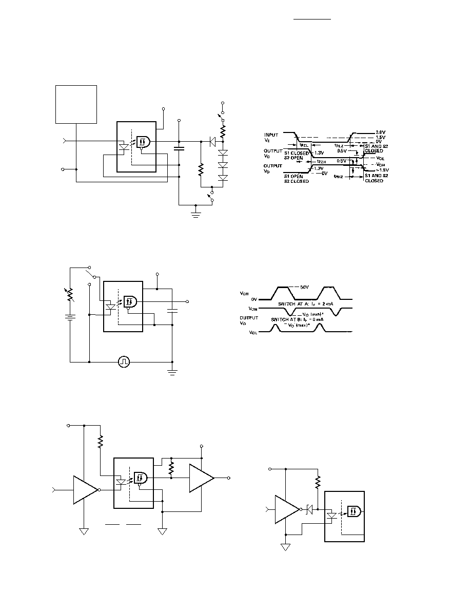
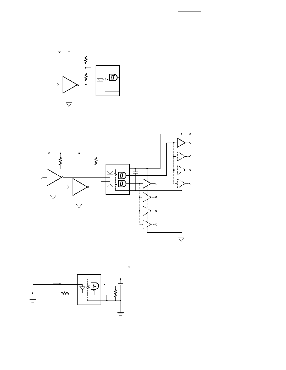
Figure 10. LSTTL to CMOS Interface Circuit.
Figure 11. Recommended LED Drive Circuit.
GND
VCC
D.U.T.
RL
665
VCC1
(+5 V)
VCC2
(4.5 TO 20 V)
CMOS
TOTEM
POLE
OUTPUT
GATE
VO
VE
DATA
OUTPUT
TTL OR
LSTTL
2
DATA
INPUT
1
VCC2
5 V
10 V
15 V
20 V
RL
1.1 K
2.37 K
3.83 K
5.11 K
GND
VCC
D.U.T.
750
VCC1
(+5 V)
TOTEM
POLE
OUTPUT
GATE
TTL OR
LSTTL
DATA
INPUT
Figure 9. Test Circuit for Common Mode Transient Immunity and Typical Waveforms.
Figure 8. Test Circuit for t
PHZ
, t
PZH
, t
PLZ
, and t
PZL
.
*SEE NOTE 6.
11
Figure 13. Recommended LSTTL to LSTTL Circuit.
Figure 14. Single Channel Operating Circuit for Burn-in and Steady State Life Tests.
GND
VCC
VE
D.U.T.*
*ALL CHANNELS TESTED SIMULTANEOUSLY.
CONDITIONS: IF = 8 mA
VCC + 20 V
VIN
+
≠
IF
IO = -14 mA
0.01 µF
TA = +125 ∞C
1.90 V
100
IO
1200
GND
VCC
D.U.T.
619
VCC1
(+5 V)
OPEN
COLLECTOR
GATE
TTL OR
LSTTL
DATA
INPUT
4.02 K
Figure 12. Series LED Drive with Open Collector Gate
(4.02 k
Resistor Shunts I
OH
from the LED).
GND
VCC
D.U.T.
665
VCC1
(+5 V)
TOTEM
POLE
OUTPUT
GATE
TTL OR
LSTTL
DATA
INPUT
TTL OR
LSTTL
DATA
INPUT
665
TOTEM
POLE
OUTPUT
GATE
1
1
2
0.1
µF
DATA
OUTPUT
VCC2
(+5 V)
DATA
OUTPUT
UP TO 16 LSTTL
LOADS
OR 4 TTL LOADS
UP TO 16 LSTTL
LOADS
OR 4 TTL LOADS

MIL-PRF-38534 Class H,
Class K, and DSCC SMD
Test Program
Agilent's Hi-Rel Optocouplers are
in compliance with MIL-PRF-
38534 Classes H and K. Class H
and Class K devices are also in
compliance with DSCC drawings
5962-88768 and
5962-88769.
Testing consists of 100% screen-
ing and quality conformance
inspection to MIL-PRF-38534.
www.semiconductor.agilent.com
Data subject to change.
Copyright © 1999 Agilent Technologies, Inc.
Obsoletes 5967-6330E
5980-0280E (10/00)