 | –≠–ª–µ–∫—Ç—Ä–æ–Ω–Ω—ã–π –∫–æ–º–ø–æ–Ω–µ–Ω—Ç: HCPL-5760 | –°–∫–∞—á–∞—Ç—å:  PDF PDF  ZIP ZIP |
AC/DC to Logic Interface
Hermetically Sealed
Optocouplers
Technical Data
Applications
∑ Military and Space
∑ High Reliability Systems
∑ Transportation, Medical,
and Life Critical Systems
∑ Limit Switch Sensing
∑ Low Voltage Detector
∑ ac/dc Voltage Sensing
∑ Relay Contact Monitor
∑ Relay Coil Voltage Monitor
∑ Current Sensing
∑ Microprocessor Interface
∑ Telephone Ring Detection
∑ Harsh Industrial
Environments
Features
∑ Dual Marked with Device
Part Number and DSCC
Standard Microcircuit
Drawing
∑ Manufactured and Tested
on a MIL-PRF-38534
Certified Line
∑ QML-38534, Class H and K
∑ Hermetically Sealed 8-pin
Dual In-Line Packages
∑ Performance Guaranteed
over -55
∞
C to +125
∞
C
∑ ac or dc Input
∑ Programmable Sense Voltage
∑ Hysteresis
∑ HCPL-3700 Operating
Compatibility
∑ Logic Compatible Output
∑ 1500 Vdc Withstand Test
Voltage
∑ Thresholds Guaranteed over
Temperature
∑ Thresholds Independent of
LED Characteristics
Description
These devices are single channel,
hermetically sealed, voltage/
current threshold detection
optocouplers. The products are
capable of operation and storage
over the full military temperature
range and can be purchased as
either standard product, or with
full MIL-PRF-38534 Class Level
H or K testing, or from the DSCC
Standard Microcircuit Drawing
(SMD) 5962-89477. All devices
are manufactured and tested on
a MIL-PRF-38534 certified line
and are included in the DSCC
Qualified Manufacturers List,
QML-38534 for Hybrid
Microcircuits.
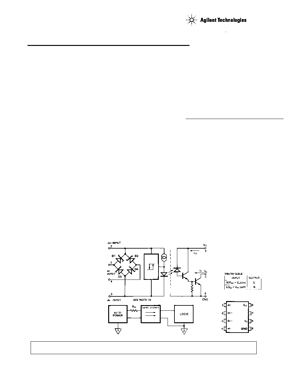
Schematic
CAUTION: It is advised that normal static precautions be taken in handling and assembly of this component to
prevent damage and/or degradation which may be induced by ESD.
HCPL-576X*
5962-8947701
*See matrix for available extensions
HCPL-5760/1/K
The connection of a 0.1
µF bypass capacitor between pins 8 and 5 is recommended.

2
Selection Guide≠Package Styles and Lead
Configuration Options
Agilent Part # and Options
Commercial
HCPL-5760
MIL-PRF-38534 Class H
HCPL-5761
MIL-PRF-38534 Class K
HCPL-576K
Standard Lead Finish
Gold
Solder Dipped
Option #200
Butt Joint/Gold Plate
Option #100
Gull Wing/Soldered
Option #300
Crew Cut/Gold Plate
Option #600
Class H SMD Part #
Prescript for all below
5962-
Either Gold or Soldered
8947701PX
Gold Plate
8947701PC
Solder Dipped
8947701PA
Butt Joint/Gold Plate
8947701YC
Butt Joint/Soldered
8947701YA
Gull Wing/Soldered
8947701XA
Crew Cut/Gold Plate
Available
Crew Cut/Soldered
Available
Class K SMD Part #
Prescript for all below
5962-
Either Gold or Soldered
8947702KPX
Gold Plate
8947702KPC
Solder Dipped
8947702KPA
Butt Joint/Gold Plate
8947702KYC
Butt Joint/Soldered
8947702KYA
Gull Wing/Soldered
8947702KXA
Crew Cut/Gold Plate
Available
Crew Cut/Soldered
Available
Each unit contains a light emit-
ting diode (LED), a threshold
sensing input buffer IC, and a
high gain photon detector to
provide an optocoupler which
permits adjustable external
threshold levels. The input buffer
circuit has a nominal turn on
threshold of 2.5 mA (I
TH+
) and
3.6 volts (V
TH+
). The addition of
one or more external attenuation
resistors permits the use of this
device over a wide range of input
voltages and currents. Threshold
sensing prior to the LED and
detector elements minimizes
effects of any variation in optical
coupling. Hysteresis is also
provided in the buffer for extra
noise immunity and switching
stability.
The buffer circuit is designed
with internal clamping diodes to
protect the circuitry and LED
from a wide range of over-voltage
and over-current transients while
the diode bridge enables easy use
with ac voltage input.
These units combine several
unique functions in a single
package, providing the user with
an ideal component for computer
input boards and other applica-
tions where a predetermined
input threshold optocoupler level
is desirable.
The high gain output stage
features an open collector output
providing both TTL compatible
saturation voltages and CMOS
compatible breakdown voltages.
This is an eight pin DIP which
may be purchased with a variety
of lead bend and plating options.
See Selection Guide Table for
details. Standard Microcircuit
Drawing (SMD) parts are
available for each lead style.
3
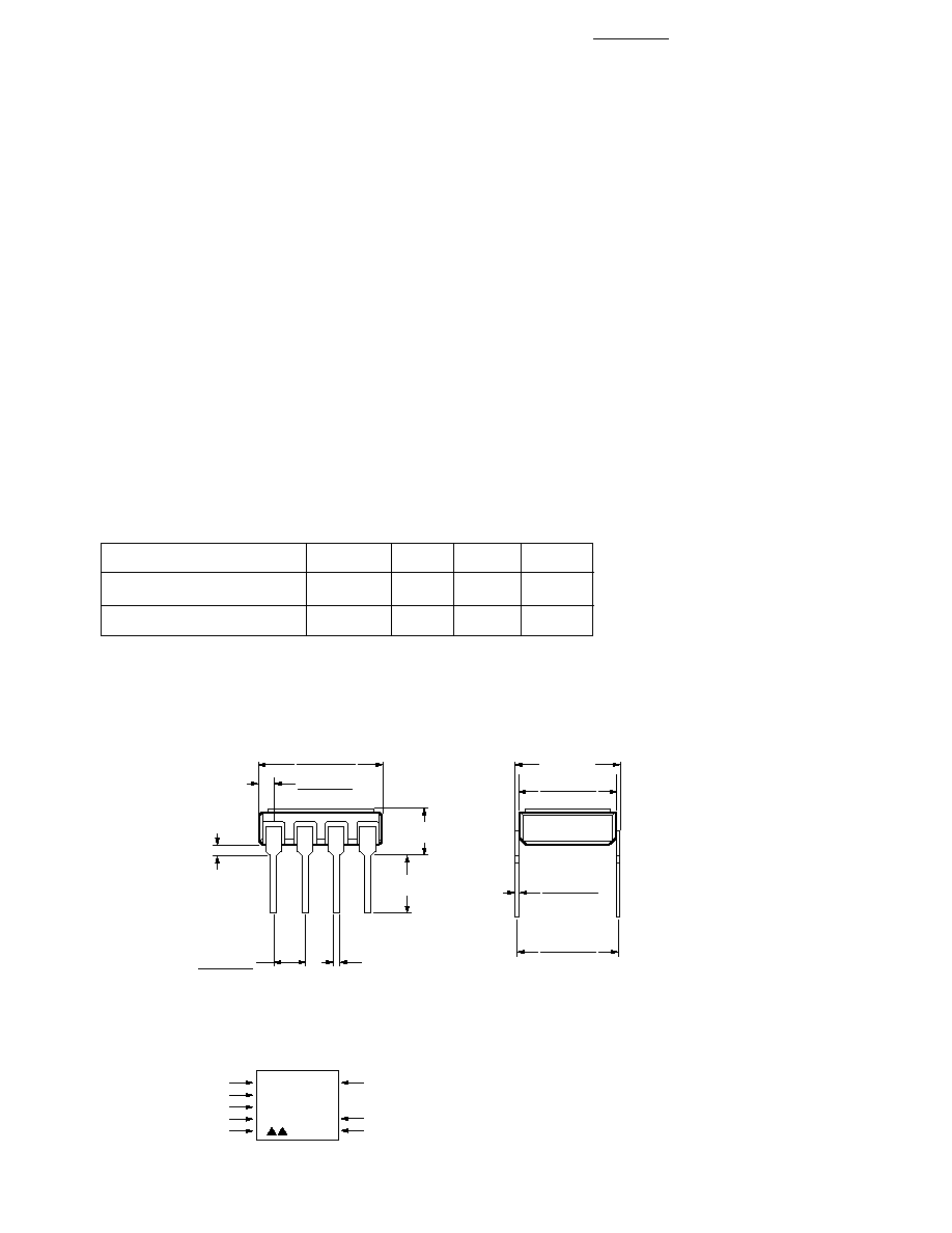
Outline Drawing
8 Pin DIP Through Hole
Device Marking
Parameter
Symbol
Min.
Max.
Units
Power Supply
V
CC
3.0
18
V
Operating Frequency
[1]
f
0
10
KHz
Recommended Operating Conditions
Absolute Maximum Ratings
Storage Temperature Range ....................................... -65
∞C to +150∞C
Operating Temperature .................................................. -55
∞C to 125∞C
Lead Solder Temperature ............................................. 260
∞C for 10 s
[2]
Average Input Current, I
IN
........................................................ 15 mA
[3]
Surge Input Current, I
IN,SG
................................................... 140 mA
[3,4]
Peak Transient Input Current, I
IN,PK
..................................... 500 mA
[3,4]
Input Power Dissipation, P
IN
................................................. 195 mW
[5]
Total Package Power Dissipation, P
d
......................................... 260 mW
Output Power Dissipation, P
O
..................................................... 65 mW
Average Output Current, I
O
.......................................................... 40 mA
Supply Voltage,V
CC
(Pins 8-5) .............................. -0.5 min., 20 V max.
Output Voltage, V
O
(Pins 6-5) ................................ -0.5 min., 20 V max.
ESD Classification
(MIL-STD-883, Method 3015) ........................................... (
), Class 2
;;
;;
;;
;;
3.81 (0.150)
MIN.
4.32 (0.170)
MAX.
9.40 (0.370)
9.91 (0.390)
0.51 (0.020)
MAX.
2.29 (0.090)
2.79 (0.110)
0.51 (0.020)
MIN.
0.76 (0.030)
1.27 (0.050)
8.13 (0.320)
MAX.
7.36 (0.290)
7.87 (0.310)
0.20 (0.008)
0.33 (0.013)
7.16 (0.282)
7.57 (0.298)
NOTE: DIMENSIONS IN MILLIMETERS (INCHES).
COMPLIANCE INDICATOR,*
DATE CODE, SUFFIX (IF NEEDED)
A QYYWWZ
XXXXXX
XXXXXXX
XXX XXX
50434
COUNTRY OF MFR.
Agilent CAGE CODE*
Agilent DESIGNATOR
DSCC SMD*
PIN ONE/
ESD IDENT
Agilent P/N
DSCC SMD*
* QUALIFIED PARTS ONLY

4
Option
Description
Hermetic Optocoupler Options
100
Surface mountable hermetic optocoupler with leads trimmed for butt joint assembly. This option
is available on commercial and hi-rel product.
200
Lead finish is solder dipped rather than gold plated. This option is available on commercial and
hi-rel product. DSCC Drawing part numbers contain provisions for lead finish.
300
Surface mountable hermetic optocoupler with leads cut and bent for gull wing assembly. This
option is available on commercial and hi-rel product. This option has solder dipped leads.
600
Surface mountable hermetic optocoupler with leads trimmed for butt joint assembly. This option
is available on commercial and hi-rel product. Contact factory for the availability of this option
on DSCC part types.
Note: Dimensions in millimeters (inches).
;;
;;
;
;;
1.14 (0.045)
1.40 (0.055)
4.32 (0.170)
MAX.
0.51 (0.020)
MAX.
2.29 (0.090)
2.79 (0.110)
0.51 (0.020)
MIN.
7.36 (0.290)
7.87 (0.310)
0.20 (0.008)
0.33 (0.013)
;
;;
;
;;
0.51 (0.020)
MIN.
4.57 (0.180)
MAX.
0.51 (0.020)
MAX.
2.29 (0.090)
2.79 (0.110)
1.40 (0.055)
1.65 (0.065)
9.65 (0.380)
9.91 (0.390)
5∞ MAX.
4.57 (0.180)
MAX.
0.20 (0.008)
0.33 (0.013)
;
;;
;
;;
3.81 (0.150)
MAX.
1.02 (0.040)
TYP.
2.29 (0.090)
2.79 (0.110)
0.51 (0.020)
MIN.
7.36 (0.290)
7.87 (0.310)
0.20 (0.008)
0.33 (0.013)
5
Group A
Parameter
Symbol
Conditions
Subgroup
Min.
Typ.*
Max.
Units
Fig.
Note
I
TH+
V
IN
= V
TH+
; V
CC
= 4.5 V;
1, 2, 3
1.75
2.5
3.20
mA
V
O
= 0.4 V; I
O
2.6 mA
Input Threshold
Current
I
TH-
V
IN
= V
TH-
; V
CC
= 4.5 V;
1, 2, 3
0.93
1.3
1.62
mA
V
O
= 2.4 V; I
OH
250 µA
V
IN
= V
2
- V
3
; Pins 1
V
TH+
& 4 Open
1, 2, 3
3.18
3.6
4.10
V
7
V
CC
= 4.5 V; V
O
= 0.4 V;
dc
I
O
2.6 mA
(Pins 2, 3)
V
IN
= V
2
- V
3
; Pins 1
V
TH-
& 4 Open
1, 2, 3
1.90
2.5
3.00
V
1, 2
V
CC
= 4.5 V; V
O
= 2.4 V;
Input
I
O
250 µA
Threshold
Voltage
V
IN
= |V
1
- V
4
|; Pins
V
TH+
2 & 3 Open
1, 2, 3
3.79
5.0
5.62
V
V
CC
= 4.5 V; V
O
= 0.4 V;
ac
I
O
2.6 mA
(Pins 1, 4)
7, 8
V
IN
= |V
1
- V
4
|; Pins 2
V
TH-
& 3 Open
1, 2, 3
2.57
3.7
4.52
V
V
CC
= 4.5 V; V
O
= 2.4 V;
I
O
250 µA
V
IHC1
= V
2
- V
3
;
V
IHC1
V
3
= GND;
1, 2, 3
5.3
5.9
7.5
V
I
IN
= 10 mA; Pin 1 & 4
Connected to Pin 3
V
IHC2
= |V
1
- V
4
|;
Input Clamp Voltage
V
IHC2
|I
IN
| = 10 mA;
1, 2, 3
6.0
6.6
8.0
V
3
15
Pins 2 & 3 Open
V
IHC3
= V
2
- V
3
;
V
3
= GND;
1, 2, 3
12.0
14.0
V
V
IHC3
I
IN
= 13.5 mA;
Pins 1 & 4 Open
Input Current
I
IN
V
IN
= V
2
- V
3
= 5.0 V;
1, 2, 3
3.0
3.9
4.5
mA
4
Pins 1 & 4 Open
Logic Low
V
OL
V
CC
= 4.5 V;
1, 2, 3
0.05
0.4
V
4
Output Voltage
I
OL
= 2.6 mA
Logic High
I
OH
V
OH
= V
CC
= 18 V
1, 2, 3
250
µA
Output Current
7
Logic Low
I
CCL
V
2
- V
3
= 5.0 V;
1, 2, 3
0.8
3.0
mA
Supply Current
V
O
= Open; V
CC
= 18 V
Logic High
I
CCH
V
CC
= 18 V; V
O
= Open
1, 2, 3
0.001
20
µA
5
Supply Current
45% RH, t = 5 s;
Input-Output
I
I-O
V
I-O
= 1500 Vdc;
1
1
µA
9, 10
Insulation
T
A
= 25
∞C
Electrical Characteristics
T
A
= -55
∞C to 125∞C, unless otherwise specified. See note 16.