AC/DC to Logic Interface
Hermetically Sealed
Optocouplers
Technical Data
Applications
∑ Military and Space
∑ High Reliability Systems
∑ Transportation, Medical,
and Life Critical Systems
∑ Limit Switch Sensing
∑ Low Voltage Detector
∑ ac/dc Voltage Sensing
∑ Relay Contact Monitor
∑ Relay Coil Voltage Monitor
∑ Current Sensing
∑ Microprocessor Interface
∑ Telephone Ring Detection
∑ Harsh Industrial
Environments
Features
∑ Dual Marked with Device
Part Number and DSCC
Standard Microcircuit
Drawing
∑ Manufactured and Tested
on a MIL-PRF-38534
Certified Line
∑ QML-38534, Class H and K
∑ Hermetically Sealed 8-pin
Dual In-Line Packages
∑ Performance Guaranteed
over -55
∞
C to +125
∞
C
∑ ac or dc Input
∑ Programmable Sense Voltage
∑ Hysteresis
∑ HCPL-3700 Operating
Compatibility
∑ Logic Compatible Output
∑ 1500 Vdc Withstand Test
Voltage
∑ Thresholds Guaranteed over
Temperature
∑ Thresholds Independent of
LED Characteristics
Description
These devices are single channel,
hermetically sealed, voltage/
current threshold detection
optocouplers. The products are
capable of operation and storage
over the full military temperature
range and can be purchased as
either standard product, or with
full MIL-PRF-38534 Class Level
H or K testing, or from the DSCC
Standard Microcircuit Drawing
(SMD) 5962-89477. All devices
are manufactured and tested on
a MIL-PRF-38534 certified line
and are included in the DSCC
Qualified Manufacturers List,
QML-38534 for Hybrid
Microcircuits.
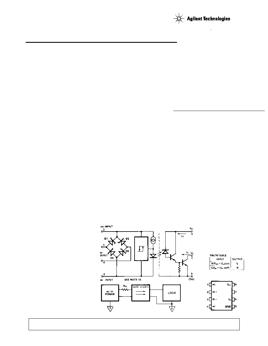
Schematic
CAUTION: It is advised that normal static precautions be taken in handling and assembly of this component to
prevent damage and/or degradation which may be induced by ESD.
HCPL-576X*
5962-8947701
*See matrix for available extensions
HCPL-5760/1/K
The connection of a 0.1
µF bypass capacitor between pins 8 and 5 is recommended.

2
Selection Guide≠Package Styles and Lead
Configuration Options
Agilent Part # and Options
Commercial
HCPL-5760
MIL-PRF-38534 Class H
HCPL-5761
MIL-PRF-38534 Class K
HCPL-576K
Standard Lead Finish
Gold
Solder Dipped
Option #200
Butt Joint/Gold Plate
Option #100
Gull Wing/Soldered
Option #300
Crew Cut/Gold Plate
Option #600
Class H SMD Part #
Prescript for all below
5962-
Either Gold or Soldered
8947701PX
Gold Plate
8947701PC
Solder Dipped
8947701PA
Butt Joint/Gold Plate
8947701YC
Butt Joint/Soldered
8947701YA
Gull Wing/Soldered
8947701XA
Crew Cut/Gold Plate
Available
Crew Cut/Soldered
Available
Class K SMD Part #
Prescript for all below
5962-
Either Gold or Soldered
8947702KPX
Gold Plate
8947702KPC
Solder Dipped
8947702KPA
Butt Joint/Gold Plate
8947702KYC
Butt Joint/Soldered
8947702KYA
Gull Wing/Soldered
8947702KXA
Crew Cut/Gold Plate
Available
Crew Cut/Soldered
Available
Each unit contains a light emit-
ting diode (LED), a threshold
sensing input buffer IC, and a
high gain photon detector to
provide an optocoupler which
permits adjustable external
threshold levels. The input buffer
circuit has a nominal turn on
threshold of 2.5 mA (I
TH+
) and
3.6 volts (V
TH+
). The addition of
one or more external attenuation
resistors permits the use of this
device over a wide range of input
voltages and currents. Threshold
sensing prior to the LED and
detector elements minimizes
effects of any variation in optical
coupling. Hysteresis is also
provided in the buffer for extra
noise immunity and switching
stability.
The buffer circuit is designed
with internal clamping diodes to
protect the circuitry and LED
from a wide range of over-voltage
and over-current transients while
the diode bridge enables easy use
with ac voltage input.
These units combine several
unique functions in a single
package, providing the user with
an ideal component for computer
input boards and other applica-
tions where a predetermined
input threshold optocoupler level
is desirable.
The high gain output stage
features an open collector output
providing both TTL compatible
saturation voltages and CMOS
compatible breakdown voltages.
This is an eight pin DIP which
may be purchased with a variety
of lead bend and plating options.
See Selection Guide Table for
details. Standard Microcircuit
Drawing (SMD) parts are
available for each lead style.
3
Outline Drawing
8 Pin DIP Through Hole
Device Marking
Parameter
Symbol
Min.
Max.
Units
Power Supply
V
CC
3.0
18
V
Operating Frequency
[1]
f
0
10
KHz
Recommended Operating Conditions
Absolute Maximum Ratings
Storage Temperature Range ....................................... -65
∞C to +150∞C
Operating Temperature .................................................. -55
∞C to 125∞C
Lead Solder Temperature ............................................. 260
∞C for 10 s
[2]
Average Input Current, I
IN
........................................................ 15 mA
[3]
Surge Input Current, I
IN,SG
................................................... 140 mA
[3,4]
Peak Transient Input Current, I
IN,PK
..................................... 500 mA
[3,4]
Input Power Dissipation, P
IN
................................................. 195 mW
[5]
Total Package Power Dissipation, P
d
......................................... 260 mW
Output Power Dissipation, P
O
..................................................... 65 mW
Average Output Current, I
O
.......................................................... 40 mA
Supply Voltage,V
CC
(Pins 8-5) .............................. -0.5 min., 20 V max.
Output Voltage, V
O
(Pins 6-5) ................................ -0.5 min., 20 V max.
ESD Classification
(MIL-STD-883, Method 3015) ........................................... (
), Class 2
;;
;;
;;
;;
3.81 (0.150)
MIN.
4.32 (0.170)
MAX.
9.40 (0.370)
9.91 (0.390)
0.51 (0.020)
MAX.
2.29 (0.090)
2.79 (0.110)
0.51 (0.020)
MIN.
0.76 (0.030)
1.27 (0.050)
8.13 (0.320)
MAX.
7.36 (0.290)
7.87 (0.310)
0.20 (0.008)
0.33 (0.013)
7.16 (0.282)
7.57 (0.298)
NOTE: DIMENSIONS IN MILLIMETERS (INCHES).
COMPLIANCE INDICATOR,*
DATE CODE, SUFFIX (IF NEEDED)
A QYYWWZ
XXXXXX
XXXXXXX
XXX XXX
50434
COUNTRY OF MFR.
Agilent CAGE CODE*
Agilent DESIGNATOR
DSCC SMD*
PIN ONE/
ESD IDENT
Agilent P/N
DSCC SMD*
* QUALIFIED PARTS ONLY
4
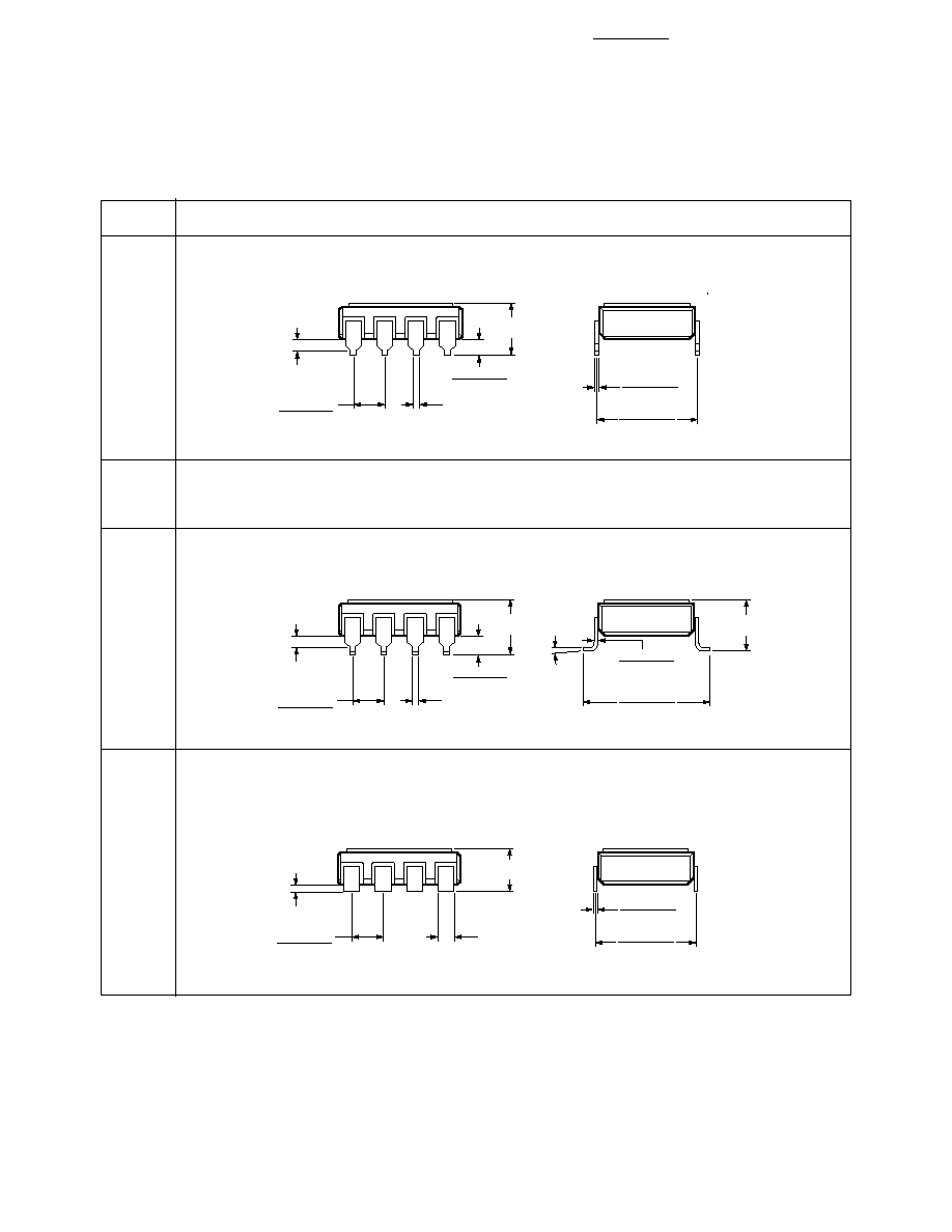
Option
Description
Hermetic Optocoupler Options
100
Surface mountable hermetic optocoupler with leads trimmed for butt joint assembly. This option
is available on commercial and hi-rel product.
200
Lead finish is solder dipped rather than gold plated. This option is available on commercial and
hi-rel product. DSCC Drawing part numbers contain provisions for lead finish.
300
Surface mountable hermetic optocoupler with leads cut and bent for gull wing assembly. This
option is available on commercial and hi-rel product. This option has solder dipped leads.
600
Surface mountable hermetic optocoupler with leads trimmed for butt joint assembly. This option
is available on commercial and hi-rel product. Contact factory for the availability of this option
on DSCC part types.
Note: Dimensions in millimeters (inches).
;;
;;
;
;;
1.14 (0.045)
1.40 (0.055)
4.32 (0.170)
MAX.
0.51 (0.020)
MAX.
2.29 (0.090)
2.79 (0.110)
0.51 (0.020)
MIN.
7.36 (0.290)
7.87 (0.310)
0.20 (0.008)
0.33 (0.013)
;
;;
;
;;
0.51 (0.020)
MIN.
4.57 (0.180)
MAX.
0.51 (0.020)
MAX.
2.29 (0.090)
2.79 (0.110)
1.40 (0.055)
1.65 (0.065)
9.65 (0.380)
9.91 (0.390)
5∞ MAX.
4.57 (0.180)
MAX.
0.20 (0.008)
0.33 (0.013)
;
;;
;
;;
3.81 (0.150)
MAX.
1.02 (0.040)
TYP.
2.29 (0.090)
2.79 (0.110)
0.51 (0.020)
MIN.
7.36 (0.290)
7.87 (0.310)
0.20 (0.008)
0.33 (0.013)

5
Group A
Parameter
Symbol
Conditions
Subgroup
Min.
Typ.*
Max.
Units
Fig.
Note
I
TH+
V
IN
= V
TH+
; V
CC
= 4.5 V;
1, 2, 3
1.75
2.5
3.20
mA
V
O
= 0.4 V; I
O
2.6 mA
Input Threshold
Current
I
TH-
V
IN
= V
TH-
; V
CC
= 4.5 V;
1, 2, 3
0.93
1.3
1.62
mA
V
O
= 2.4 V; I
OH
250 µA
V
IN
= V
2
- V
3
; Pins 1
V
TH+
& 4 Open
1, 2, 3
3.18
3.6
4.10
V
7
V
CC
= 4.5 V; V
O
= 0.4 V;
dc
I
O
2.6 mA
(Pins 2, 3)
V
IN
= V
2
- V
3
; Pins 1
V
TH-
& 4 Open
1, 2, 3
1.90
2.5
3.00
V
1, 2
V
CC
= 4.5 V; V
O
= 2.4 V;
Input
I
O
250 µA
Threshold
Voltage
V
IN
= |V
1
- V
4
|; Pins
V
TH+
2 & 3 Open
1, 2, 3
3.79
5.0
5.62
V
V
CC
= 4.5 V; V
O
= 0.4 V;
ac
I
O
2.6 mA
(Pins 1, 4)
7, 8
V
IN
= |V
1
- V
4
|; Pins 2
V
TH-
& 3 Open
1, 2, 3
2.57
3.7
4.52
V
V
CC
= 4.5 V; V
O
= 2.4 V;
I
O
250 µA
V
IHC1
= V
2
- V
3
;
V
IHC1
V
3
= GND;
1, 2, 3
5.3
5.9
7.5
V
I
IN
= 10 mA; Pin 1 & 4
Connected to Pin 3
V
IHC2
= |V
1
- V
4
|;
Input Clamp Voltage
V
IHC2
|I
IN
| = 10 mA;
1, 2, 3
6.0
6.6
8.0
V
3
15
Pins 2 & 3 Open
V
IHC3
= V
2
- V
3
;
V
3
= GND;
1, 2, 3
12.0
14.0
V
V
IHC3
I
IN
= 13.5 mA;
Pins 1 & 4 Open
Input Current
I
IN
V
IN
= V
2
- V
3
= 5.0 V;
1, 2, 3
3.0
3.9
4.5
mA
4
Pins 1 & 4 Open
Logic Low
V
OL
V
CC
= 4.5 V;
1, 2, 3
0.05
0.4
V
4
Output Voltage
I
OL
= 2.6 mA
Logic High
I
OH
V
OH
= V
CC
= 18 V
1, 2, 3
250
µA
Output Current
7
Logic Low
I
CCL
V
2
- V
3
= 5.0 V;
1, 2, 3
0.8
3.0
mA
Supply Current
V
O
= Open; V
CC
= 18 V
Logic High
I
CCH
V
CC
= 18 V; V
O
= Open
1, 2, 3
0.001
20
µA
5
Supply Current
45% RH, t = 5 s;
Input-Output
I
I-O
V
I-O
= 1500 Vdc;
1
1
µA
9, 10
Insulation
T
A
= 25
∞C
Electrical Characteristics
T
A
= -55
∞C to 125∞C, unless otherwise specified. See note 16.
6
Group A
Parameter
Symbol
Conditions
Subgroup
Min.
Typ.*
Max.
Units
Fig.
Note
Propagation Delay
Time to Logic Low
t
PHL
R
L
=1.8 k
, C
L
= 15 pF
9, 10, 11
4
20
µs
6, 11
Output Level
6, 7
Propagation Delay
Time to Logic High
t
PLH
R
L
=1.8 k
, C
L
= 15 pF
9, 10, 11
8
40
µs
6, 12
Output Level
Logic High Common
V
CM
= 50 V
T
A
= 25
∞C
9
1000
10,000
Mode Transient
|CM
H
|
I
IN
= 0 mA
V/
µs
Immunity
V
CM
= 450 V
10,000
13,
8
14,
Logic Low Common
V
CM
= 50 V
T
A
= 25
∞C
9
1000
5,000
17
Mode Transient
|CM
L
|
I
IN
= 4 mA
V/
µs
Immunity
V
CM
= 250 V
5,000
*All typical values are at T
A
= 25
∞C, V
CC
= 5 V unless otherwise noted.
Electrical Characteristics
T
A
= -55
∞C to 125∞C, V
CC
= 5.0 V, unless otherwise specified (continued).
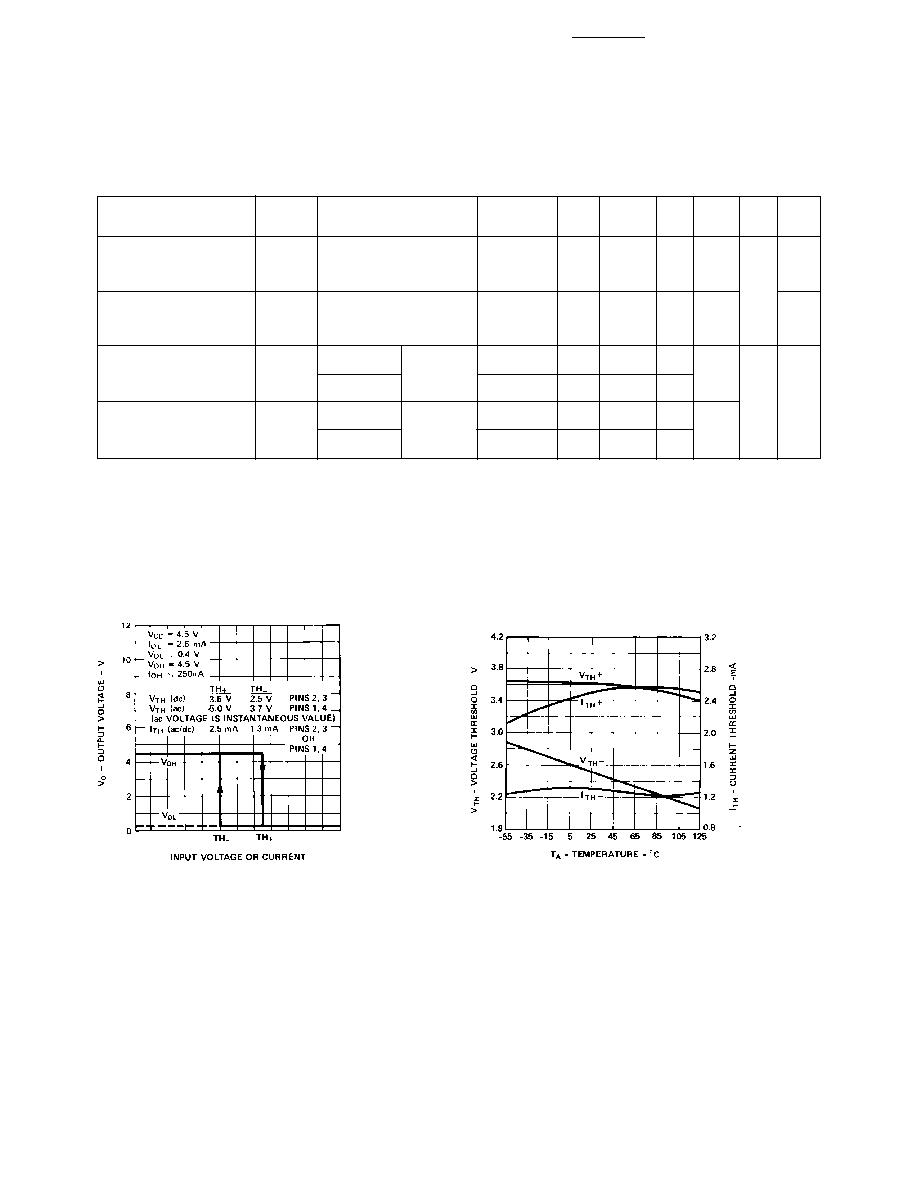
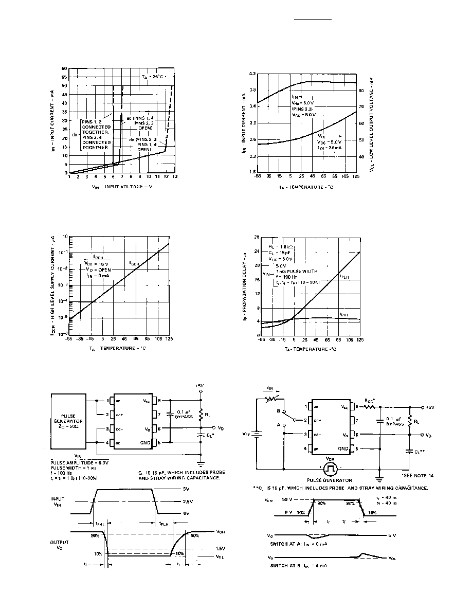
Figure 1. Typical Transfer Characteristics.
Figure 2. Typical dc Threshold Levels vs. Temperature.

7
Parameter
Symbol
Typ.
Units
Conditions
Fig.
Note
I
HYS
1.2
mA
I
HYS
= I
TH+
- I
TH-
Hysteresis
1
V
HYS
1.1
V
V
HYS
= V
TH+
- V
TH-
Input Clamp Voltage
V
ILC
-0.76
V
V
ILC
= V
2
- V
3
; V
3
= GND;
I
IN
= -10 mA
Bridge Diode
V
D1,2
0.62
I
IN
= 3 mA (see schematic)
Forward Voltage
V
D3,4
0.73
Input-Output Resistance
R
I-O
10
12
V
I-O
= 500 Vdc
9
Input-Output Capacitance
C
I-O
2.0
pF
f = 1 MHz, V
I-O
= 0 Vdc
Input Capacitance
C
IN
50
pF
f = 1 MHz; V
IN
= 0 V,
Pins 2 & 3, Pins 1 & 4 Open
Output Rise Time
t
r
10
µs
7
(10-90%)
Output Fall Time
t
f
0.5
µs
7
(90-10%)
Typical Characteristics
All typical values are at T
A
= 25
∞C, V
CC
= 5 V, unless otherwise specified.
Notes:
1. Maximum operating frequency is
defined when output waveform (Pin 6)
attains only 90% of V
CC
with R
L
= 1.8
k
, C
L
= 15 pF using a 5 V square
wave input signal.
2. Measured at a point 1.6 mm below
seating plane.
3. Current into/out of any single lead.
4. Surge input current duration is 3 ms at
120 Hz pulse repetition rate. Transient
input current duration is 10
µs at
120 Hz pulse repetition rate. Note that
maximum input power, P
IN
, must be
observed.
5. Derate linearly above 100
∞C free-air
temperature at a rate of 4.26 mW/
∞C.
Maximum input power dissipation of
195 mW allows an input IC junction
temperature of 150
∞C at an ambient
temperature of T
A
= 125
∞C with a
typical thermal resistance from
junction to ambient of
JA
i
= 235
∞C/W.
The typical thermal resistance from
junction to case is equal to 170
∞C/W.
Excessive P
IN
and T
J
may result in
device degradation.
6. The 1.8 k
load represents 1 TTL unit
load of 1.6 mA and the 4.7 k
pull-up
resistor.
7. Logic low output level at Pin 6 occurs
under the conditions of V
IN
V
TH+
as
well as the range of V
IN
> V
TH
≠ once
V
IN
has exceeded V
TH+
. Logic high
output level at Pin 6 occurs under the
conditions of V
IN
V
TH-
as well as the
range of V
IN
< V
TH+
once V
IN
has
decreased below V
TH-
.
8. The ac voltage is instantaneous
voltage.
9. Device considered a two terminal
device: Pins 1, 2, 3, 4 connected
together, Pins 5, 6, 7 8 connected
together.
10. This is a momentary withstand test,
not an operating condition.
11. The t
PHL
propagation delay is
measured from the 2.5 V level of the
leading edge of a 5.0 V input pulse (1
µs rise time) to the 1.5 V level on the
leading edge of the output pulse (see
Figure 7).
12. The t
PLH
propagation delay is
measured from the 2.5 V level of the
trailing edge of a 5.0 V input pulse (1
µs fall time) to the 1.5 V level on the
trailing edge of the output pulse (see
Figure 7).
13. Common mode transient immunity in
Logic High level is the maximum
tolerable dV
CM/dt
of the common mode
voltage, V
CM
, to ensure that the output
will remain in a Logic High state (i.e.,
V
O
> 2.0 V). Common mode transient
immunity in Logic Low level is the
maximum tolerable dV
CM/dt
of the
common mode voltage, V
CM
, to ensure
that the output will remain in a Logic
Low state (i.e., V
O
< 0.8 V). See
Figure 8.
14. In applications where dV
CM/dt
may
exceed 50,000 V/
µs (such as static
discharge), a series resistor, R
CC
,
should be included to protect the
detector IC from destructively high
surge currents. The recommended
value for R
CC
is 240
per volt of
allowable drop in V
CC
(between Pin 8
and V
CC
) with a minimum value of
240
.
15. D
1
and D
2
are Schottky diodes; D
3
and D
4
are zener diodes.
16. Standard parts receive 100% testing at
25
∞C (Subgroups 1 and 9). SMD,
Class H and Class K parts receive
100% testing at 25, 125, and -55
∞C
(Subgroups 1 and 9, 2 and 10 ,3 and
11, respectively.)
17. Parameters shall be tested as part of
device initial characterization and after
process changes. Parameters shall be
guaranteed to the limits specified for
all lots not specifically tested.
8
Figure 7. Switching Test Circuit.
Figure 8. Test Circuit for Common Mode Transient
Immunity and Typical Waveforms.
Figure 3. Typical Input Characteristics, I
IN
vs. V
IN
.
(AC Voltage is Instantaneous Value.)
Figure 4. Typical Input Current, I
IN
, and Low Level Output
Voltage, V
OL
, vs. Temperature.
Figure 5. Typical High Level Supply Current, I
CCH
vs.
Temperature.
Figure 6. Typical Propagation Delay vs. Temperature.
HCPL-5760/1/K
HCPL-5760/1/K
9
Electrical Considerations
The HCPL-5760, HCPL-5761,
HCPL-576K or 5962-89477
optocoupler has internal
temperature compensated,
predictable voltage and current
threshold points which allow
selection of an external resistor,
R
x
, to determine larger external
threshold voltage levels. For a
desired external threshold
voltage, V
±
, a corresponding
typical value of R
x
can be
obtained from Figure 10. Specific
calculation of R
x
can be obtained
from Equation (1) of Figure 11.
Specification of both V
+
and V
-
voltage threshold levels simulta-
neously can be obtained by the
use of R
x
and R
p
as shown in
Figure 11 and determined by
Equations (2) and (3).
R
x
can provide over-current
transient protection by limiting
input current during a transient
condition. For monitoring
contacts with a relay or switch,
the HCPL-5760/1/K, or
5962-89477 combination with R
x
and R
p
can be used to allow a
specific current to be conducted
through the contacts for cleaning
purposes (wetting current).
The choice of which input voltage
clamp level to choose depends
upon the application of this
device (see Figure 3). It is
recommended that the low clamp
condition be used when possible
to lower the input power
dissipation as well as the LED
current, which minimizes LED
degradation over time.
In applications where dV
CM/dt
may
be extremely large (such as static
discharge), a series resistor, R
CC
,
should be connected in series
with V
CC
and Pin 8 to protect the
Figure 10. Typical External Threshold
Characteristic, V
±
vs. R
x
.
detector IC from destructively
high surge currents. See note 14
for determination of R
CC
. In
addition, it is recommended that a
ceramic disc bypass capacitor of
0.01
µF to 0.1 µF be placed
between Pins 8 and 5 to reduce
the effect of power supply noise.
For interfacing ac signals to TTL
systems, output low pass filtering
can be performed with a pullup
resistor of 1.5 k
and 20 µF
capacitor. This application
requires a Schmitt trigger gate to
avoid slow rise time chatter
problems. For ac input applica-
tions, a filter capacitor can be
placed across the dc input
terminals for either signal or
transient filtering.
Either ac (Pins 1, 4) or dc (Pins
2, 3) input can be used to
determine external threshold
levels.
For one specifically selected
external threshold voltage level
V
+
or V
-
, R
x
can be determined
without use of R
p
via
V
+
- V
TH+
(-) (-)
R
x
= ≠≠≠≠≠≠≠≠≠
(1)
I
TH+
(-)
See Application Note 1004 for
more information.
For two specifically selected
external threshold voltage levels,
V
+
and V
-
, the use of R
x
and R
p
will permit this selection via
equations (2), (3) provided the
following conditions are met:
R
P
=
V
TH-
(V
+
) - V
TH+
(V
-
)
≠≠≠≠≠≠≠≠≠≠≠≠≠≠≠≠≠≠≠≠≠≠≠≠≠≠≠ (3)
I
TH+
(V
-
- V
TH-
) + I
TH-
(V
TH+
- V
+
)
V
TH-
(V
+
) - V
TH+
(V
-
)
R
x
= ≠≠≠≠≠≠≠≠≠≠≠≠≠≠≠≠≠≠≠≠ (2)
I
TH+
(V
TH-
) - I
TH-
(V
TH+
)
V
+
V
TH+
V
+
- V
TH+
I
TH+
≠≠≠
≠≠≠ and ≠≠≠≠≠≠≠≠ < ≠≠≠≠
V
-
V
TH-
V
-
- V
TH-
I
TH-
Figure 9. Operating Circuit for Burn-In and Steady State Life Tests.

MIL-PRF-38534 Class H,
Class K, and DSCC SMD
Test Program
Agilent Technologies' Hi-Rel
Optocouplers are in compliance
with MIL-PRF-38534 Class H and
K. Class H and Class K devices
are also in compliance with DSCC
drawing 5962-89477.
Testing consists of 100% screen-
ing and quality conformance
inspection to MIL-PRF-38534.
Figure 11. External Threshold Voltage Level Selection.
HCPL-5760/1/K
10

www.semiconductor.agilent.com
Data subject to change.
Copyright © 2001 Agilent Technologies
August 23, 2001
Obsoletes 5968-9404E (11/00)
5988-3093EN