 | –≠–ª–µ–∫—Ç—Ä–æ–Ω–Ω—ã–π –∫–æ–º–ø–æ–Ω–µ–Ω—Ç: HCPL-7520 | –°–∫–∞—á–∞—Ç—å:  PDF PDF  ZIP ZIP |

Agilent HCPL-7520
Isolated Linear Sensing IC
Data Sheet
Description
The HCPL-7520 isolated linear
current sensing IC family is
designed for current sensing in
low-power electronic motor
drives. In a typical implementa-
tion, motor current flows through
an external resistor and the
resulting analog voltage drop is
sensed by the HCPL-7520. An
output voltage is created on the
other side of the HCPL-7520
optical isolation barrier. This
single-ended output voltage is
proportional to the motor
current. Since common-mode
voltage swings of several hundred
volts in tens of nanoseconds are
common in modern switching
inverter motor drives, the HCPL-
7520 was designed to ignore very
high common-mode transient
slew rates (of at least 10 kV/
µs).
The high CMR capability of the
HCPL-7520 isolation amplifier
provides the precision and
stability needed to accurately
monitor motor current in high
noise motor control environ-
ments, providing for smoother
control (less "torque ripple") in
various types of motor control
applications.
Features
∑ 15 kV/
µs common-mode rejection
at Vcm = 1000 V
∑ Compact, auto-insertable 8-pin
DIP package
∑ 60 ppm/
∞C gain drift vs.
temperature
∑ ≠0.6 mV input offset voltage
∑ 8
µV/∞C input offset voltage vs.
temperature
∑ 100 kHz bandwidth
∑ 0.06% nonlinearity, single-ended
amplifer oon
∑ Worldwide safety approval:
UL 1577 (3750 Vrms/1 min.) and
CSA (pending), DIN EN 60747-5-2
(Option #060 only pending)
∑ Advanced sigma-delta (
-)
A/D converter technology
Applications
∑ Low-power inverter current
sensing
∑ Motor phase and rail current
sensing
∑ Switched mode power supply
signal isolation
∑ General purpose low-power
current sensing and monitoring
∑ General purpose analog signal
isolation
The product can also be used for
general analog signal isolation
applications. For general
applications, we recommend the
HCPL-7520 (gain tolerance of
±5%). The HCPL-7520 utilizes
sigma delta (
-) analog-to-
digital converter technology to
delivery offset and gain accuracy
and stability over time and
temperature. This performance is
delivered in a compact, auto-
insert, 8-pin DIP package that
meets worldwide regulatory
safety standards. (A gull-wing
surface mount option #300 is
also available).
CAUTION: It is advised that normal static precautions be taken in handling and assembly of this
component to prevent damage and /or degradation which may be induced by ESD.
1
2
3
4
8
7
6
5
IDD1
VDD1
VIN+
VIN≠
GND1
IDD2
VDD2
VOUT
VREF
GND2
+
≠
+
≠
SHIELD
Functional Diagram
2
Ordering Information
Specify part number followed by option number (if desired).
Example:
HCPL-7520-XXX
No option = Standard DIP package, 50 per tube.
300 = Gull Wing Surface Mount Option, 50 per tube.
500 = Tape and Reel Packaging Option.
060 = DIN EN 60747-5-2 Option.
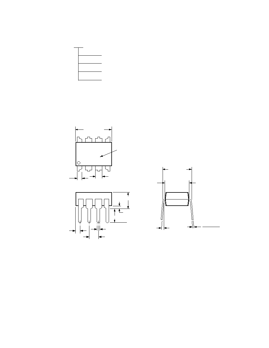
Package Outline Drawings
HCPL-7520 Standard DIP Package
9.80 ± 0.25
(0.386 ± 0.010)
1.78 (0.070) MAX.
1.19 (0.047) MAX.
A 7520
YYWW
DATE CODE
1.080 ± 0.320
(0.043 ± 0.013)
2.54 ± 0.25
(0.100 ± 0.010)
0.51 (0.020) MIN.
0.65 (0.025) MAX.
4.70 (0.185) MAX.
2.92 (0.115) MIN.
DIMENSIONS IN MILLIMETERS AND (INCHES).
5
6
7
8
4
3
2
1
5∞ TYP.
0.20 (0.008)
0.33 (0.013)
7.62 ± 0.25
(0.300 ± 0.010)
6.35 ± 0.25
(0.250 ± 0.010)

3
HCPL-7520 Gull Wing Surface Mount Option 300 Outline Drawing
Solder Reflow Temperature Profile
0
TIME (SECONDS)
TEMPERATURE (
∞
C)
200
100
50
150
100
200
250
300
0
30
SEC.
50 SEC.
30
SEC.
160∞C
140∞C
150∞C
PEAK
TEMP.
245∞C
PEAK
TEMP.
240∞C
PEAK
TEMP.
230∞C
SOLDERING
TIME
200∞C
PREHEATING TIME
150∞C, 90 + 30 SEC.
2.5∞C ± 0.5∞C/SEC.
3∞C + 1∞C/≠0.5∞C
TIGHT
TYPICAL
LOOSE
ROOM
TEMPERATURE
PREHEATING RATE 3∞C + 1∞C/≠0.5∞C/SEC.
REFLOW HEATING RATE 2.5∞C ± 0.5∞C/SEC.
0.635 ± 0.25
(0.025 ± 0.010)
12∞ NOM.
0.20 (0.008)
0.33 (0.013)
9.65 ± 0.25
(0.380 ± 0.010)
0.635 ± 0.130
(0.025 ± 0.005)
7.62 ± 0.25
(0.300 ± 0.010)
5
6
7
8
4
3
2
1
9.80 ± 0.25
(0.386 ± 0.010)
6.350 ± 0.25
(0.250 ± 0.010)
1.016 (0.040)
1.194 (0.047)
1.194 (0.047)
1.778 (0.070)
9.398 (0.370)
9.960 (0.390)
4.826
(0.190)
TYP.
0.381 (0.015)
0.635 (0.025)
PAD LOCATION (FOR REFERENCE ONLY)
1.080 ± 0.320
(0.043 ± 0.013)
4.19
(0.165)
MAX.
1.780
(0.070)
MAX.
1.19
(0.047)
MAX.
2.54
(0.100)
BSC
DIMENSIONS IN MILLIMETERS (INCHES).
TOLERANCES (UNLESS OTHERWISE SPECIFIED): xx.xx = 0.01
xx.xxx = 0.005
A 7520
YYWW
LEAD COPLANARITY
MAXIMUM: 0.102 (0.004)

4
Regulatory Information
The HCPL-7520 is pending
approval by the following
organizations:
DIN EN
Pending approval under DIN EN
60747-5-2 with V
IORM
= 891 V
PEAK
.
DIN EN 60747-5-2 Insulation Characteristics
[1]
Description
Symbol
Characteristic Unit
Installation classification per DIN EN 0110-1/1997-04, Table 1
for rated mains voltage
150 V
rms
I ≠ IV
for rated mains voltage
300 V
rms
I ≠ III
for rated mains voltage
600 V
rms
I ≠ II
Climatic Classification
55/100/21
Pollution Degree (DIN EN 0110-1/1997-04)
2
Maximum Working Insulation Voltage
V
IORM
891
V
peak
Input to Output Test Voltage, Method b
[2]
V
IORM
x 1.875 = V
PR
, 100% production test with t
m
= 1 sec, partial discharge <5 pC
V
PR
1670
V
peak
Input to Output Test Voltage, Method a
[2]
V
IORM
x 1.5 = V
PR
, type and sample test, t
m
= 60 sec, partial discharge <5 pC
V
PR
1336
V
peak
Highest Allowable Overvoltage (transient overvoltage t
ini
= 10 sec)
V
IOTM
6000
V
peak
Safety-limiting values ≠ maximum values allowed in the event of a failure.
Case Temperature
T
S
175
∞C
Input Current
[3]
I
S, INPUT
400
mA
Output Power
[3]
P
S, OUTPUT
600
mW
Insulation Resistance at T
S
, V
IO
= 500 V
R
S
>10
9
Notes:
1. Insulation characteristics are guaranteed only within the safety maximum ratings which must be ensured by protective circuits within the
application. Surface Mount Classifications is Class A in accordance with CECC00802.
2. Refer to the optocoupler section of the Isolation and Control Components Designer's Catalog, under Product Safety Regulations section, (DIN EN
60747-5-2) for a detailed description of Method a and Method b partial discharge test profiles.
3. Refer to the following figure for dependence of P
S
and I
S
on ambient temperature.
UL
Pending approval under UL 1577,
component recognition program
up to V
ISO
= 3750 V
RMS
expected
prior to product release. File
E55361.
CSA
Pending approval under CSA
Component Acceptance Notice
#5, File CA 88324 expected prior
to product release.
OUTPUT POWER
≠
P
S
, INPUT CURRENT
≠
I
S
0
0
TS ≠ CASE TEMPERATURE ≠ ∞C
200
600
400
25
800
50
75 100
200
150 175
PS (mW)
125
100
300
500
700
IS (mA)

5
Insulation and Safety Related Specifications
Parameter
Symbol
Value
Unit
Conditions
Minimum External Air Gap
L(101)
7.4
mm
Measured from input terminals to output terminals,
(clearance)
shortest distance through air.
Minimum External Tracking
L(102)
8.0
mm
Measured from input terminals to output terminals,
(creepage)
shortest distance path along body.
Minimum Internal Plastic Gap
0.5
mm
Through insulation distance conductor to conductor,
(internal clearance)
usually the straight line distance thickness between the
emitter and detector.
Tracking Resistance
CTI
>175
V
DIN IEC 112 Part 1
(comparative tracking index)
Isolation Group
IIIa
Material Group (DIN EN 0110-1/1997-04)
Absolute Maximum Ratings
Parameter
Symbol
Min.
Max.
Units
Note
Storage Temperature
T
S
≠55
125
∞C
Operating Temperature
T
A
≠40
100
∞C
Supply Voltage
V
DD1_max
, V
DD1_max
0
6
V
Steady-State Input Voltage
V
IN+
, V
IN-
≠2.0
V
DD1
+ 0.5
-
V
Two Second Transient Input Voltage
V
IN+
, V
IN-
≠6.0
V
DD1
+ 0.5
-
V
Output Voltage
V
OUT
≠0.5
V
DD2
+ 0.5
-
V
Reference Input Voltage
V
REF
0.0
V
DD2
+ 0.5
-
V
Reference Input Current
I
REF
20
-
mA
Lead Solder Temperature
260
∞C for 10 sec., 1.6 mm below seating plane
Solder Reflow Temperature Profile
See Package Outline Drawings section
Recommended Operating Conditions
Parameter
Symbol
Min.
Max.
Units
Note
Operating Temperature
T
A
≠40
85
∞C
Supply Voltage
V
DD1
, V
DD2
4.5
5.5
V
Input Voltage (accurate and linear)
V
IN+
, V
IN-
≠200
200
mV
Input Voltage (functional)
V
IN+
, V
IN-
≠2.0
2.0
V
Reference Input Voltage
V
REF
4.0
V
DD2
V