 | –≠–ª–µ–∫—Ç—Ä–æ–Ω–Ω—ã–π –∫–æ–º–ø–æ–Ω–µ–Ω—Ç: HCPL-7840 | –°–∫–∞—á–∞—Ç—å:  PDF PDF  ZIP ZIP |
1-248
H
CAUTION: It is advised that normal static precautions be taken in handling and assembly of this component to
prevent damage and/or degradation which may be induced by ESD.
HCPL-7840
Analog Isolation Amplifier
Technical Data
A 0.1 F bypass capacitor must be connected between pins 1 and 4 and between pins 5 and 8.
Features
∑ High Common Mode
Rejection (CMR): 15 kV/
µ
s
at V
CM
= 1000 V
∑ 5% Gain Tolerance
∑ 0.1% Nonlinearity
∑ Low Offset Voltage and Off-
set Temperature Coefficient
∑ 100 kHz Bandwidth
∑ Performance Specified Over
-40
∞
C to 85
∞
C Temperature
Range
∑ Recognized Under UL 1577
and CSA Approved for
Dielectric Withstand Proof
Test Voltage of 2500 Vac, 1
Minute
∑ Standard 8-Pin DIP Package
Applications
∑ Motor Phase and Rail
Current Sensing
∑ Inverter Current Sensing
∑ Switched Mode Power
Supply Signal Isolation
∑ General Purpose Current
Sensing and Monitoring
∑ General Purpose Analog
Signal Isolation
Description
The HCPL-7840 isolation ampli-
fier provides accurate, electrically
isolated and amplified representa-
tions of voltage and current.
When used with a shunt resistor
in the current path, the HCPL-
7840 offers superior reliability,
cost effectiveness, size and
autoinsertability compared with
the traditional solutions such as
current transformers and Hall-
effect sensors.
The HCPL-7840 consists of a
sigma-delta analog-to-digital
converter optically coupled to a
digital-to-analog converter.
Superior performance in design
critical specifications such as
common-mode rejection, offset
voltage, nonlinearity, operating
temperature range and regulatory
compliance make the HCPL-7840
the clear choice for designing
reliable, lower-cost, reduced-size
products such as motor
controllers and inverters.
Common-mode rejection of
15 kV/
µ
s makes the HCPL-7840
suitable for noisy electrical
environments such as those
generated by the high switching
rates of power IGBTs.
Low offset voltage together with
a low offset voltage temperature
coefficient permits accurate use
of auto-calibration techniques.
Gain tolerance of 5% with 0.1%
nonlinearity further provide the
performance necessary for
accurate feedback and control.
A wide operating temperature
range with specified performance
allows the HCPL-7840 to be used
in hostile industrial environments.
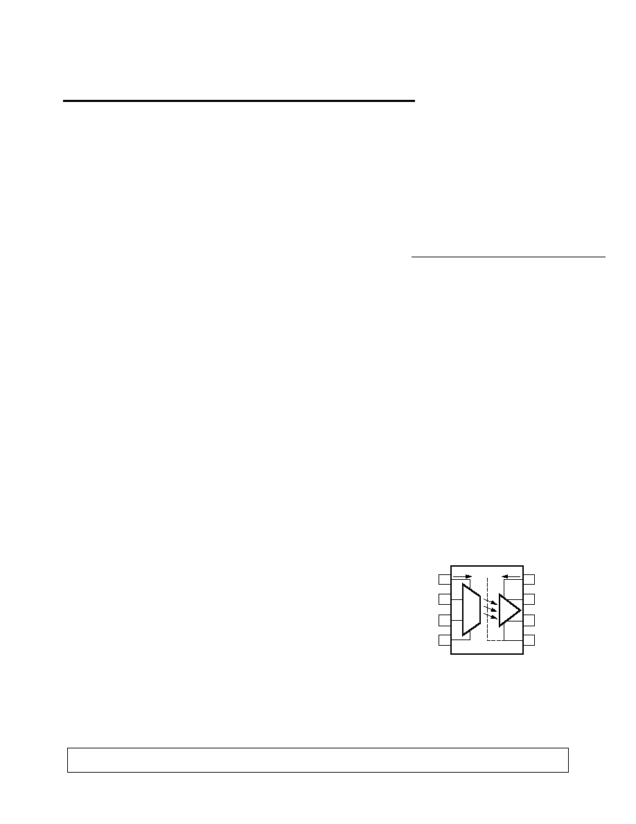
Functional Diagram
1
2
3
4
8
7
6
5
IDD1
VDD1
VIN+
VIN≠
GND1
IDD2
VDD2
VOUT+
VOUT≠
GND2
+
≠
+
≠
SHIELD
5965-4784E
1-249
Package Outline Drawings
Standard DIP Package
9.65 ± 0.25
(0.380 ± 0.010)
1.78 (0.070) MAX.
1.19 (0.047) MAX.
HP 7840
YYWW
DATE CODE
1.080 ± 0.320
(0.043 ± 0.013)
2.54 ± 0.25
(0.100 ± 0.010)
0.51 (0.020) MIN.
0.65 (0.025) MAX.
4.70 (0.185) MAX.
2.92 (0.115) MIN.
7.62 ± 0.25
(0.300 ± 0.010)
5∞ TYP.
5
6
7
8
4
3
2
1
6.35 ± 0.25
(0.250 ± 0.010)
0.20 (0.008)
0.33 (0.013)
0.635 ± 0.25
(0.025 ± 0.010)
12∞ NOM.
0.20 (0.008)
0.33 (0.013)
9.65 ± 0.25
(0.380 ± 0.010)
0.635 ± 0.130
(0.025 ± 0.005)
7.62 ± 0.25
(0.300 ± 0.010)
5
6
7
8
4
3
2
1
9.65 ± 0.25
(0.380 ± 0.010)
6.350 ± 0.25
(0.250 ± 0.010)
1.016 (0.040)
1.194 (0.047)
1.194 (0.047)
1.778 (0.070)
9.398 (0.370)
9.960 (0.390)
4.826
(0.190)
TYP.
0.381 (0.015)
0.635 (0.025)
PAD LOCATION (FOR REFERENCE ONLY)
1.080 ± 0.320
(0.043 ± 0.013)
4.19
(0.165)
MAX.
1.780
(0.070)
MAX.
1.19
(0.047)
MAX.
2.54
(0.100)
BSC
DIMENSIONS IN MILLIMETERS (INCHES).
TOLERANCES (UNLESS OTHERWISE SPECIFIED): xx.xx = 0.01
xx.xxx = 0.005
HP 7840
YYWW
LEAD COPLANARITY
MAXIMUM: 0.102 (0.004)
Gull Wing Surface Mount Option 300
Ordering Information
HCPL-7840#xxx
No option = Standard DIP Package, 50 per tube
300 = Gull Wing Surface Mount Lead Option, 50 per tube
500 = Tape/Reel Package Option (1 K min.), 1000 per reel
Option data sheets available. Contact your Hewlett-Packard sales representative or authorized distributor for
more information.
1-250
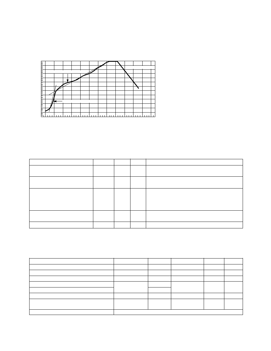
Maximum Solder Reflow Thermal Profile
Regulatory Information
The HCPL-7840 has been
approved by the following
organizations:
UL Recognized under UL 1577,
Component Recognition
Program, File E55361.
CSA Approved under CSA
Component Acceptance Notice
#5, File CA 88324.
240
T = 115∞C, 0.3∞C/SEC
0
T = 100∞C, 1.5∞C/SEC
T = 145∞C, 1∞C/SEC
TIME ≠ MINUTES
TEMPERATURE ≠ ∞C
220
200
180
160
140
120
100
80
60
40
20
0
260
1
2
3
4
5
6
7
8
9
10
11
12
(NOTE: USE OF NON-CHLORINE ACTIVATED FLUXES IS RECOMMENDED.)
Insulation and Safety Related Specifications
Parameter
Symbol
Value
Units
Conditions
Min. External Air Gap
L(IO1)
7.1
mm
Measured from input terminals to output
(External Clearance)
terminals, shortest distance through air.
Min. External Tracking Path
L(IO2)
7.4
mm
Measured from input terminals to output
(External Creepage)
terminals, shortest distance path along body.
Min. Internal Plastic Gap
0.08
mm
Through insulation distance, conductor to
(Internal Clearance)
conductor, usually the direct distance
between the photoemitter and photodetector
inside the optocoupler cavity.
Tracking Resistance
CTI
200
Volts
DIN IEC 112/VDE 0303 Part 1
(Comparative Tracking Index)
Isolation Group
IIIa
Material Group (DIN VDE 0110, 1/89, Table 1)
Option 300 - surface mount classification is Class A in accordance with CECC 00802.
Absolute Maximum Ratings
Parameter
Symbol
Min.
Max.
Unit
Note
Storage Temperature
T
S
-55
125
∞
C
Ambient Operating Temperature
T
A
-40
85
∞
C
Supply Voltages
V
DD1
, V
DD2
0.0
5.5
V
Steady-State Input Voltage
V
IN+
,
V
IN-
-2.0
V
DD1
+0.5
V
1
2 Second Transient Input Voltage
-6.0
Output Voltages
V
OUT+
,
V
OUT-
-0.5
V
DD2
+0.5
V
Lead Solder Temperature
T
LS
260
∞
C
(10 sec., 1.6 mm below seating plane)
Solder Reflow Temperature Profile
See Maximum Solder Reflow Thermal Profile Section
1-251
DC Electrical Specifications
All specifications, typicals and figures are at the nominal operating conditions of V
IN+
= 0 V, V
IN-
= 0 V,
T
A
= 25
∞
C, V
DD1
= 5 V and V
DD2
= 5 V, unless otherwise noted.
Parameter
Symbol
Min.
Typ. Max. Unit
Test Conditions
Fig.
Note
Input Offset Voltage
V
OS
-1.2
-0.2
1.0
mV
1
2
-3.0
-0.2
2.0
-40
∞
C
T
A
85
∞
C
1,2,3
4.5
(V
DD1
, V
DD2
)
5.5 V
Gain
G
7.60
8.00
8.40
V/V
-200
V
IN+
200 mV
5
7.44
8.00
8.56
-200
V
IN+
200 mV
5,6,7
-40
∞
C
T
A
85
∞
C
4.5
(V
DD1
, V
DD2
)
5.5 V
200 mV Nonlinearity
NL
200
0.1
0.2
%
-200
V
IN+
200 mV
5, 8
3
0.4
-200
V
IN+
200 mV
5,8,9
-40
∞
C
T
A
85
∞
C
10,12
4.5
(V
DD1
, V
DD2
)
5.5 V
100 mV Nonlinearity
NL
100
0.05
0.1
-100
V
IN+
100 mV
5, 8
0.2
-100
V
IN+
100 mV
5,8,9
-40
∞
C
T
A
85
∞
C
11,12
4.5
(V
DD1
, V
DD2
)
5.5 V
Maximum Input Voltage
|V
IN+
| 320
mV
4
Before Output Clipping
Average Input Bias Current
I
IN
-0.57
µ
A
13
4
Average Input Resistance
R
IN
480
k
Input DC Common-Mode
CMRR
IN
69
dB
5
Rejection Ratio
Output Resistance
R
O
1
Output Low Voltage
V
OL
1.28
V
V
IN+
= 400 mV
4
6
Output High Voltage
V
OH
3.84
V
V
IN+
= -400 mV
Output Common-Mode
V
OCM
2.20
2.56
2.80
V
-400 < V
IN+
< 400 mV
Voltage
Input Supply Current
I
DD1
8.7
15.5
mA
14
Output Supply Current
I
DD2
8.8
14.5
mA
15
Output Short-Circuit Current
|I
OSC
|
11
mA
V
OUT
= 0 V or V
DD2
7
-40
∞
C
T
A
85
∞
C
4.5
(V
DD1
, V
DD2
)
5.5 V
MAX
Recommended Operating Conditions
Parameter
Symbol
Min.
Max.
Unit
Note
Ambient Operating Temperature
T
A
-40
85
∞
C
Supply Voltages
V
DD1
, V
DD2
4.5
5.5
V
Input Voltage
V
IN+
,V
IN-
-200
200
mV
1
1-252
AC Electrical Specifications
All specifications, typicals and figures are at the nominal operating conditions of V
IN+
= 0 V, V
IN-
= 0 V,
T
A
= 25
∞
C, V
DD1
= 5 V and V
DD2
= 5 V, unless otherwise noted.
Parameter
Symbol
Min.
Typ.
Max.
Unit
Test Conditions
Fig.
Note
Common Mode
CMR
10
15
kV/
µ
s
V
CM
= 1 kV
16
8
Rejection
4.5
(V
DD1
, V
DD2
)
5.5 V
Common Mode
CMRR
>140
dB
9
Rejection Ratio
at 60 Hz
Propagation Delay
t
PD50
3.7
6.5
µ
s
V
IN+
= 0 to 100 mV step
17, 18
to 50%
-40
∞
C
T
A
85
∞
C
4.5
(V
DD1
, V
DD2
)
5.5 V
Propagation Delay
t
PD90
5.7
9.9
to 90%
Rise/Fall Time
t
R/F
3.4
6.6
(10-90%)
Small-Signal
f
-3 dB
50
100
kHz
-40
∞
C
T
A
85
∞
C
17, 19,
Bandwidth
4.5
(V
DD1
, V
DD2
)
5.5 V
20
(-3 dB)
Small-Signal
f
-45
∞
33
Bandwidth (-45
∞
)
RMS Input-
V
N
0.6
mV
rms
In recommended
21, 23
10
Referred Noise
application circuit
Power Supply
PSR
570
mV
P-P
11
Rejection
Package Characteristics
All specifications, typicals and figures are at the nominal operating conditions of V
IN+
= 0 V, V
IN-
= 0 V,
T
A
= 25
∞
C, V
DD1
= 5 V and V
DD2
= 5 V, unless otherwise noted.
Parameter
Symbol
Min.
Typ.
Max.
Unit
Test Conditions
Fig.
Note
Input-Output Momentary
V
ISO
2500
V
rms
t = 1 min., RH
50%
12,13
Withstand Voltage*
Input-Output Resistance
R
I-O
10
12
V
I-O
= 500 Vdc
13
Input-Output Capacitance
C
I-O
0.6
pF
f = 1 MHz
V
I-O
= 0 Vdc
*The Input-Output Momentary Withstand Voltage is a dielectric voltage rating that should not be interpreted as an input-output
continuous voltage rating. For the continuous voltage rating, refer to the VDE 0884 Insulation Characteristics Table (if applicable),
your equipment level safety specification, or HP Application Note 1074, "Optocoupler Input-Output Endurance Voltage."