Hermetically Sealed Analog
Isolation Amplifier
Technical Data
HCPL-7850
HCPL-7851
5962-97557
Features
∑ Performance Guaranteed
over Full Military
Temperature Range: ≠55∞C
to +125∞C
∑ Manufactured and Tested on
a MIL-PRF-38534 Certified
Line
∑ Hermetically Sealed
Packages
∑ Dual Marked with Device
Part Number and DSCC
Drawing Number
∑ QML-38534, Class H
∑ HCPL-7840 Function
Compatibility
∑ High Common Mode
Rejection (CMR):
8 kV/
µ
s at VCM = 1000 V
∑ 5% Gain Tolerance
∑ 0.1% Nonlinearity
∑ Low Offset Voltage and
Offset Temperature
Coefficient
∑ 100 kHz Bandwidth
Applications
∑ Industrial and Military
∑ High Reliability Systems
∑ Harsh Industrial
Environments
∑ Transportation, Medical,
and Life Critical Systems
∑ General Purpose Analog
Signal Isolation
∑ Motor Phase and Rail
Current Sensing
∑ Inverter Current Sensing
∑ Switched Mode Power
Supply Signal Isolation
∑ General Purpose Current
Sensing and Monitoring
Description
The HCPL-7850/7851 is an
isolation amplifier that provides
accurate, electrically isolated and
amplified representations of
voltage and current. When used
with a shunt resistor to monitor
the motor phase current in a high
speed motor drive, the device will
offer superior reliability
compared with the traditional
solutions such as current
transformers and Hall-effect
sensors. The HCPL-7850/7851
consists of a sigma-delta analog-
to-digital converter optically
coupled to a digital-to-analog
converter in a hermetically sealed
package. The products are
capable of operation and storage
over the full military temperature
range and can be purchased as
either commercial product or
with full MIL-PRF-38534 Class H
testing or from the appropriate
DSCC drawing. All devices are
manufactured and tested on a
MIL-PRF-38534 certified line and
are included in the DSCC
Qualified Manufacturers List,
QML-38534 for Hybrid
Microcircuits.
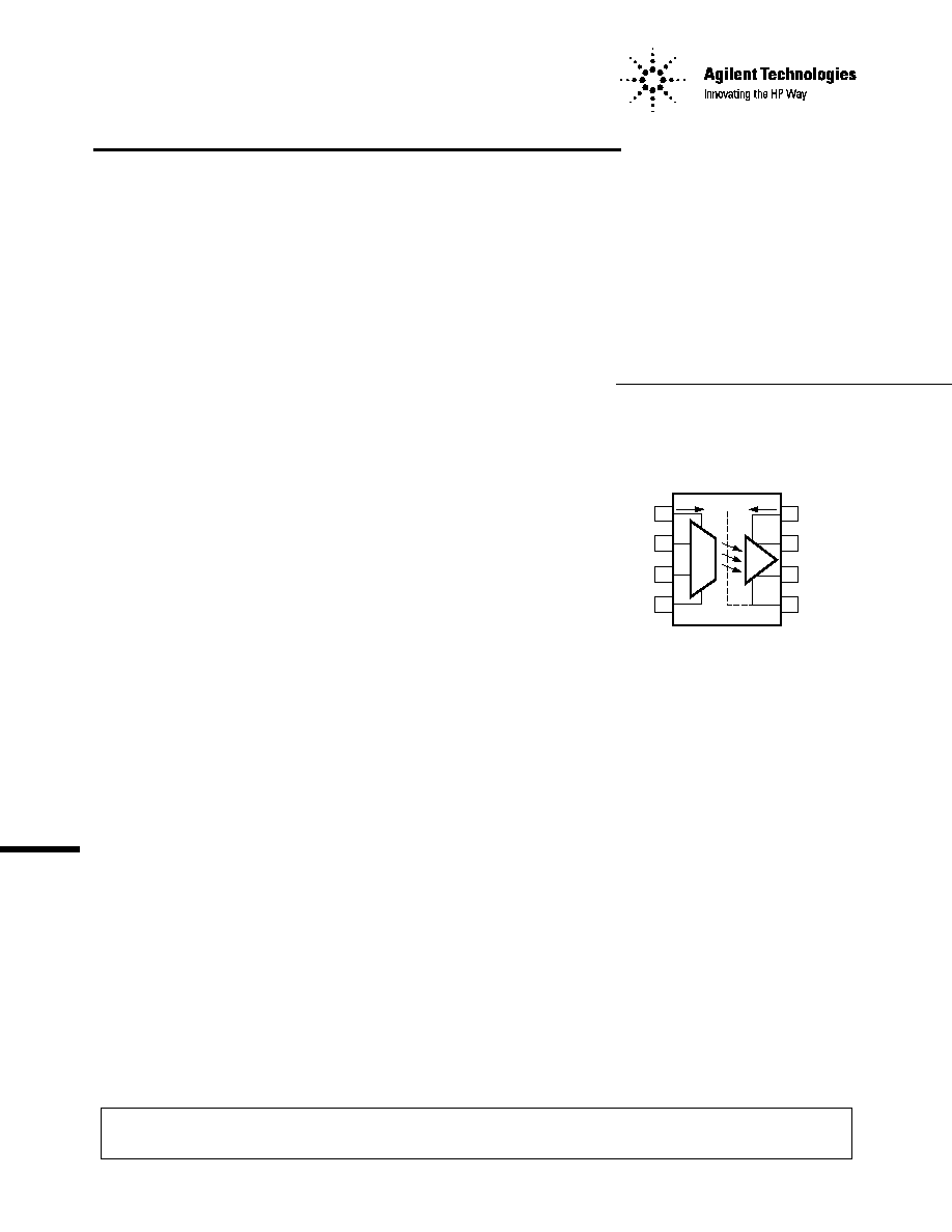
Schematic Diagram
A 0.1 F bypass capacitor must be connected between pins 1 and 4 and between pins 5 and 8.
CAUTION: It is advised that normal static precautions be taken in handling and assembly of this
component to prevent damage and/or degradation which may be induced by ESD.
1
2
3
4
8
7
6
5
IDD1
VDD1
VIN+
VIN≠
GND1
IDD2
VDD2
VOUT+
VOUT≠
GND2
+
≠
+
≠
SHIELD
2
Superior performance in design
critical specifications such as
common-mode rejection, offset
voltage, nonlinearity, and
operating temperature make the
HCPL-7850/7851 an excellent
choice for designing reliable
products such as motor
controllers and inverters.
Common-mode rejection of
8 kV/
µ
s makes the HCPL-7850/
7851 suitable for noisy electrical
environments such as those
generated by the high switching
rates of power IGBTs.
Low offset voltage together with
a low offset voltage temperature
coefficient permits accurate use
of auto-calibration techniques.
Gain tolerance of 5% with 0.1%
nonlinearity further provide the
performance necessary for
accurate feedback and control.
Selection Guide-Package Styles and Lead
Configuration Options
Agilent Part Number and Options
Commercial
HCPL-7850
MIL-PRF-38534, Class H
HCPL-7851
Standard Lead Finish
Gold Plate
Solder Dipped
Option #200
Butt Cut/Gold Plate
Option #100
Gull Wing/Soldered
Option #300
SMD Part Number
Prescript for all below
5962-
Either Gold or Solder
9755701HPX
Gold Plate
9755701HPC
Solder Dipped
9755701HPA
Butt Cut/Gold Plate
9755701HYC
Butt Cut/Soldered
9755701HYA
Gull Wing/Soldered
9755701HXA
Device Marking
COMPLIANCE INDICATOR,*
DATE CODE, SUFFIX (IF NEEDED)
A QYYWWZ
XXXXXXXX
XXXXXXXXX
XXX XXX
50434
COUNTRY OF MFR.
Agilent CAGE CODE*
Agilent DESIGNATOR
DSCC SMD*
PIN ONE/
ESD IDENT
Agilent P/N
DSCC SMD*
* QUALIFIED PARTS ONLY
3
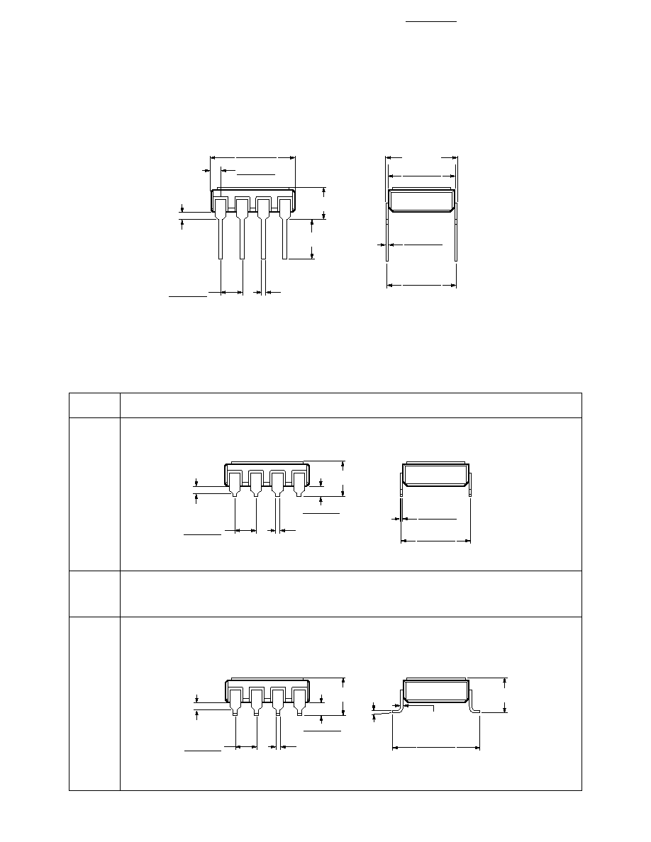
Outline Drawing
Option
Description
Hermetic Optocoupler Options
100
Surface mountable hermetic optocoupler with leads trimmed for butt joint assembly. This option
is available on commercial and hi-rel product in 8 pin DIP (see drawings below for details).
200
Lead finish is solder dipped rather than gold plated. This option is available on commercial and
hi-rel product in 8 pin DIP. DSCC Drawing part numbers contain provisions for lead finish.
300
Surface mountable hermetic optocoupler with leads cut and bent for gull wing assembly. This
option is available on commercial and hi-rel product in 8 pin DIP (see drawings below for
details). This option has solder dipped leads.
3.81 (0.150)
MIN.
4.32 (0.170)
MAX.
9.40 (0.370)
9.91 (0.390)
0.51 (0.020)
MAX.
2.29 (0.090)
2.79 (0.110)
0.51 (0.020)
MIN.
0.76 (0.030)
1.27 (0.050)
8.13 (0.320)
MAX.
7.36 (0.290)
7.87 (0.310)
0.20 (0.008)
0.33 (0.013)
7.16 (0.282)
7.57 (0.298)
NOTE: DIMENSIONS IN MILLIMETERS (INCHES).
1.14 (0.045)
1.40 (0.055)
4.32 (0.170)
MAX.
0.51 (0.020)
MAX.
2.29 (0.090)
2.79 (0.110)
0.51 (0.020)
MIN.
7.36 (0.290)
7.87 (0.310)
0.20 (0.008)
0.33 (0.013)
NOTE: DIMENSIONS IN MILLIMETERS (INCHES).
0.51 (0.020)
MIN.
5.57 (0.180)
MAX.
0.51 (0.020)
MAX.
2.29 (0.090)
2.79 (0.110)
1.40 (0.055)
1.65 (0.065)
9.65 (0.380)
9.91 (0.390)
5∞ MAX.
5.57 (0.180)
MAX.
0.20 (0.008)
0.33 (0.013)
NOTE: DIMENSIONS IN MILLIMETERS (INCHES).
4
Absolute Maximum Ratings
Storage Temperature (T
S
) ............................................. ≠65 to +150∞C
Operating Temperature (T
A
) .......................................... ≠55 to +125∞C
Supply Voltages (V
DD1
, V
DD2
) ......................................... 0.0 to +5.5 V
Steady-State Input Voltage (V
IN+
, V
IN≠
) ...... ≠2.0 V to V
DD1
+0.5 V (1/)
2 Second Transient Input Voltage ...... ≠6.0 V to V
DD1
+0.5 V (1/)
Output Voltages (V
OUT+
, V
OUT≠
) ...........................≠0.5 to V
DD2
+0.5 V
Lead Soldering Temperature (soldering, 10 seconds max.) ...... +260∞C
ESD Classification
(MIL-STD-883, Method 3015)
HCPL-7850/7851 ..... (v); Class 1
Recommended Operating Conditions
Parameter
Symbol
Min.
Max.
Units
Supply Voltages
V
DD1
,
4.5
5.5
Volts
V
DD2
Input Voltage (See Note 1)
V
IN+
,
≠200
+200
mV
V
IN≠

5
DC Electrical Specifications
Over recommended operating conditions (T
A
= ≠55∞C to +125∞C, V
IN+
= 0 V, V
IN≠
= 0 V, V
DD1
= 5 V and
V
DD2
= 5 V, unless otherwise specified).
Group A
[12]
Parameter
Symbol
Subgroups
Min.
Typ.* Max. Units
Test Conditions
Fig. Note
Input Offset
V
OS
1,2,3
≠1.0
0.6
5.0
mV
4.5 V
V
DD1
, V
DD2
)
1,2,
2
Voltage
5.5 V
3
Gain
G
2,3
7.36
8.00
8.64
V/V
≠200 mV
V
IN+
200 mV 5,6,
4.5 V
(V
DD1
, V
DD2
)
7
5.5 V
1
7.60
8.00
8.4
200 mV
NL
200
2,3
0.05
0.8
%
≠200 mV
V
IN+
200 mV 5,8,
3
Nonlinearity
4.5 V
(V
DD1
, V
DD2
)
9,10,
5.5 V
12
1
0.05
0.2
100 mV
NL
100
2,3
0.01
0.2
≠100 mV
V
IN+
100 mV 5,8,
Nonlinearity
4.5 V
(V
DD1
, V
DD2
)
9,11,
5.5 V
12
1
0.01
0.1
Output
V
OCM
1,2,3
2.20
2.56
2.80
V
≠400 mV
V
IN+
400 mV
Common-Mode
4.5 V
(V
DD1
, V
DD2
)
Voltage
5.5 V
Input Supply
I
DD1
1,2,3
10.7
15.5
mA
14,17
Current
Output Supply
I
DD2
1,2,3
9.4
14.5
mA
15,17
Current
Input-Output
I
I≠O
1
1.0
µ
A
RH = 45%, t = 5 sec.
11
Insulation
V
I≠O
= 1500 Vdc,
Leakage
T
A
= 25∞C
Current
Maximum
|V
IN+
|
320
mV
4,12
Input Voltage
MAX
Before Output
Clipping
Average Input
I
IN
≠0.57
µ
A
13
4
Bias Current
Average Input
R
IN
480
k
Resistance
Input DC
CMRR
IN
69
dB
5
Common-Mode
Rejection Ratio
Output
R
O
1
Resistance
Output Low
V
OL
1.28
V
V
IN+
= 400 mV
4
6
Voltage
Output High
V
OH
3.84
V
V
IN+
= ≠400 mV
Voltage
Output Short-
|I
OSC
|
11
mA
V
OUT
= 0 V or V
DD2
7
Circuit Current
Resistance
R
I≠O
10
12
V
I≠O
= 500 Vdc
11
(Input-Output)
Capacitance
C
I≠O
2.7
pF
f = 1 MHz
(Input≠Output)
V
I≠O
= 0 Vdc
*All typicals are at the nominal operating conditions of V
IN+
= 0 V, V
IN≠
= 0 V, T
A
= 25∞C, V
DD1
= 5 V and V
DD2
= 5 V.
6
AC Electrical Specifications
Over recommended operating conditions (T
A
= ≠55∞C to +125∞C, V
IN+
= 0 V, V
IN≠
= 0 V, V
DD1
= 5 V and
V
DD2
= 5 V, unless otherwise specified).
Group A
[12]
Parameter
Symbol
Subgroups
Min.
Typ.* Max. Units
Test Conditions
Fig. Note
Common Mode
CMR
9
5
8
kV/
V
CM
= 1 kV
16
8,13
Rejection
µ
s
4.5 V
(V
DD1
, V
DD2
)
5.5 V, T
A
= 25∞C
Propagation
t
PD50
9,10,11
3.7
7.5
µ
s
V
IN+
= 0 to 100 mV step 18,19
Delay to 50%
4.5 V
(V
DD1
, V
DD2
)
5.5 V
Propagation
t
PD90
9,10,11
5.7
11.0
Delay to 90%
Rise/Fall
t
R/F
9,10,11
3.4
7.5
Time (10-90%)
Small-Signal
f
≠3 dB
9,10,11
45
100
kHz
4.5 V
(V
DD1
, V
DD2
)
18,20,
14
Bandwidth
5.5 V
21
(≠3 dB)
V
IN+
= 200 mVpk-pk
Small-Signal
f
≠45∞
31
Bandwidth
(≠45∞)
RMS Input-
V
N
0.6
mV
rms
In recommended
22,24
9
Referred Noise
application circuit
Power Supply
PSR
570
mV
P≠P
10
Rejection
*All typicals are at the nominal operating conditions of V
IN+
= 0 V, V
IN≠
= 0 V, T
A
= 25∞C, V
DD1
= 5 V and V
DD2
= 5 V.
Notes:
1. If V
IN≠
is brought above V
DD1
≠2 V with respect to GND1 an internal test mode may be activated. This test mode is not intended for
customer use.
2. Exact offset value is dependent on layout of external bypass capacitors. The offset value in the data sheet corresponds to Agilent's
recommended layout (see Figures 26 and 27).
3. Nonlinearity is defined as half of the peak-to-peak output deviation from the best-fit gain line, expressed as a percentage of the full-scale
differential output voltage.
4. Because of the switched capacitor nature of the sigma-delta A/D converter, time averaged values are shown.
5. CMRR
IN
is defined as the ratio of the gain for differential inputs applied between pins 2 and 3 to the gain for both common mode inputs
applied to both pins 2 and 3 with respect to pin 4.
6. When the differential input signal exceeds approximately 320 mV, the outputs will limit at the typical values shown.
7. Short-circuit current is the amount of output current generated when either output is shorted to V
DD2
or ground. Agilent does not
recommend operations under these conditions.
8. CMR (also known as IMR or Isolation Mode Rejection) specifies the minimum rate of rise of a common mode signal applied across the
isolation boundary at which small output perturbations begin to occur. These output perturbations can occur with both the rising and
falling edges of the common mode waveform and may be of either polarity. A CMR failure is defined as a perturbation exceeding 200 mV
at the output of the recommended application circuit (Figure 24). See Applications section for more information on CMR.
9. Output noise comes from two primary sources: chopper noise and sigma-delta quantization noise. Chopper noise results from chopper
stabilization of the output op-amps. It occurs at a specific frequency (typically 500 kHz) and is not attenuated by the on-chip output
filter. The on-chip filter does eliminate most, but not all, of the sigma-delta quantization noise. An external filter circuit may be easily
added to the external post-amplifier to reduce the total RMS output noise. See Applications section for more information.
10. Data sheet value is the amplitude of the transient at the differential output of the HCPL-7850 when a 1 V
P≠P
, 1 MHz square wave with
100 ns rise and fall times (measured at pins 1 and 8) is applied to both V
DD1
and V
DD2
.
11. Device considered a two-terminal device: Pins 1, 2, 3, and 4 are shorted together and pins 5, 6, 7, and 8 are shorted together.
12. Commercial parts receive 100% testing at 25∞C (Subgroups 1 and 9). Hi-Rel and SMD parts receive 100% testing at 25∞C, +125∞C and
≠55∞C (Subgroups 1 and 9, 2 and 10, 3 and 11, respectively).
13. Parameters are tested as part of device initial characterization and after design and process changes only. Parameters are guaranteed to
limits specified for all lots not specifically tested.
14. The f
-3dB
test is guaranteed by the T
RISE
test.
sine wave
7
Figure 1. Input Offset Voltage Test Circuit.
Figure 2. Input Offset Change vs.
Temperature.
Figure 3. Input Offset Change vs.
V
DD1
and V
DD2
.
Figure 4. Output Voltages vs. Input
Voltage.
0.1 µF
VDD2
VOUT
8
7
6
1
3
HCPL-7850
5
2
4
0.1 µF
10 K
10 K
VDD1
+15 V
0.1 µF
0.1 µF
-15 V
+
≠
AD624CD
GAIN = 100
0.47
µF
0.47
µF
V
OS
≠ INPUT OFFSET CHANGE ≠ mV
TA ≠ TEMPERATURE ≠ ∞C
1.0
0.5
0
-20
2.0
20
VDD1 = 5 V
VDD2 = 5 V
-0.5
1.5
-60
140
60
100
V
OS
≠ INPUT OFFSET CHANGE ≠ mV
VDD ≠ SUPPLY VOLTAGE ≠ V
0.6
0.3
4.6
0.9
4.8
5.0
5.2
TA = 25∞C
-0.3
vs. VDD1 (VDD2 = 5 V)
4.4
5.6
5.4
vs. VDD2 (VDD1 = 5 V)
0
V
O
≠ OUTPUT VOLTAGE ≠ V
VIN ≠ INPUT VOLTAGE ≠ V
2.5
2.0
1.5
-0.4
4.0
-0.2
0
0.2
VDD1 = 5 V
VDD2 = 5 V
TA = 25∞C
1.0
3.0
3.5
-0.6
0.6
0.4
POSITIVE
OUTPUT
NEGATIVE
OUTPUT
8
Figure 6. Gain Change vs.
Temperature.
Figure 7. Gain Change vs. V
DD1
and
V
DD2
.
Figure 8. Nonlinearity Error Plot vs.
Input Voltage.
Figure 5. Gain and Nonlinearity Test Circuit.
0.1 µF
VDD2
8
7
6
1
3
HCPL-7850
5
2
4
0.01 µF
10 K
10 K
+15 V
0.1 µF
0.1 µF
-15 V
+
≠
AD624CD
GAIN = 4
0.47
µF
0.47
µF
VDD1
13.2
404
VIN
VOUT
+15 V
0.1 µF
0.1 µF
-15 V
+
≠
AD624CD
GAIN = 10
10 K
0.47
µF
0.1 µF
G ≠ GAIN CHANGE ≠ %
VDD ≠ SUPPLY VOLTAGE ≠ V
0.04
0.02
4.6
0.10
4.8
5.0
5.2
TA = 25∞C
-0.06
0.06
vs. VDD1 (VDD2 = 5 V)
0.08
4.4
5.6
5.4
vs. VDD2 (VDD1 = 5 V)
0
-0.02
-0.04
NL ERROR ≠ % OF FULL SCALE
VIN+ ≠ INPUT VOLTAGE ≠ V
-0.05
-0.1
0.15
0
0.1
-0.10
0.05
200 mV ERROR
0.10
-0.2
0.2
100 mV ERROR
VDD1 = 5 V
VDD2 = 5 V
VIN≠ = 0 V
TA = 25∞C
0
G
≠ GAIN CHANGE ≠ %
TA ≠ TEMPERATURE ≠ ∞C
0
-0.10
-20
0.05
20
VDD1 = 5 V
VDD2 = 5 V
-0.20
-60
140
60
100
-0.05
-0.15
9
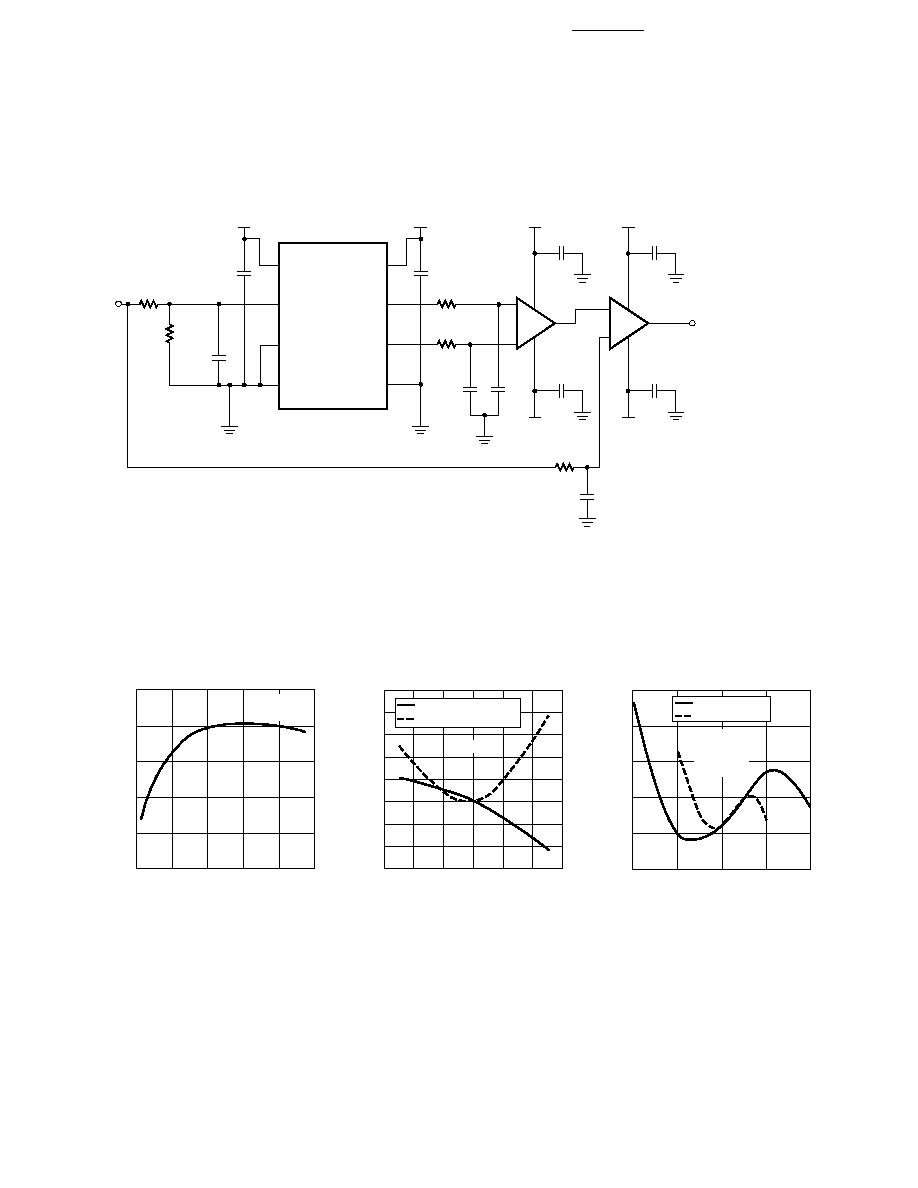
Figure 9. Nonlinearity vs.
Temperature.
Figure 10. 200 mV Nonlinearity vs.
V
DD1
and V
DD2
.
Figure 11. 100 mV Nonlinearity vs.
V
DD1
and V
DD2
.
Figure 12. Nonlinearity vs. Full-Scale
Input Voltage.
Figure 13. Input Current vs. Input
Voltage.
Figure 14. Input Supply Current vs.
Input Voltage.
NL ≠ NONLINEARITY ≠ %
TA ≠ TEMPERATURE ≠ ∞C
0.2
0.1
0.4
20
0
0.3
200 mV
-60
140
100 mV
VDD1 = 5 V
VDD2 = 5 V
VIN≠ = 0 V
TA = 25 ∞C
-20
60
100
I IN
≠ INPUT CURRENT ≠ mA
VIN+ ≠ INPUT VOLTAGE ≠ V
-4
-6
-8
-4
2
-2
0
2
VDD1 = 5 V
VDD2 = 5 V
VIN≠ = 0 V
TA = 25∞C
-10
-2
0
-6
6
4
I DD1
≠ INPUT SUPPLY CURRENT ≠ mA
VIN+ ≠ INPUT VOLTAGE ≠ V
9
11
-0.2
0
VDD1 = 5 V
VDD2 = 5 V
VIN≠ = 0 V
6
-0.4
0.4
0.2
TA = 25∞C
10
8
7
NL ≠ NONLINEARITY ≠ %
VDD ≠ SUPPLY VOLTAGE ≠ V
0.05
0.04
4.6
0.07
4.8
5.0
5.2
TA = 25∞C
0
vs. VDD1 (VDD2 = 5 V)
0.06
4.4
5.6
5.4
vs. VDD2 (VDD1 = 5 V)
NL ≠ NONLINEARITY ≠ %
VDD ≠ SUPPLY VOLTAGE ≠ V
0.015
0.010
4.6
0.025
4.8
5.0
5.2
TA = 25∞C
0.005
vs. VDD1 (VDD2 = 5 V)
0.020
4.4
5.6
5.4
vs. VDD2 (VDD1 = 5 V)
NL ≠ NONLINEARITY ≠ %
FS ≠ FULL-SCALE INPUT VOLTAGE ≠ V
0.50
5.00
±0.10
±0.20
VDD1 = 5 V
VDD2 = 5 V
0.01
0
±0.40
0.05
TA = 25∞C
±0.30
10
Figure 15. Output Supply Current vs.
Input Voltage.
Figure 16. Common Mode Rejection Test Circuit.
Figure 17. Input and Output Supply
Current vs. Temperature.
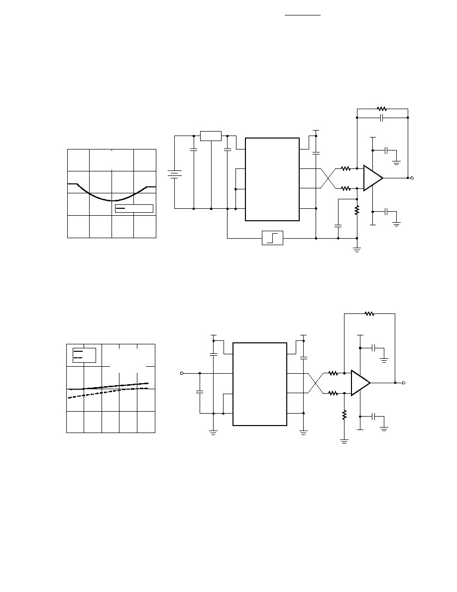
Figure 18. Propagation Delay, Rise/Fall Time and Bandwidth Test Circuit.
I DD2
≠ OUTPUT SUPPLY CURRENT ≠ mA
VIN+ ≠ INPUT VOLTAGE ≠ V
10.0
-0.2
0
VDD1 = 5 V
VDD2 = 5 V
VIN≠ = 0 V
8.0
-0.4
0.4
0.2
9.0
TA = 25∞C
9.5
8.5
0.1 µF
VDD2
VOUT
8
7
6
1
3
HCPL-7850
5
2
4
2 K
2 K
78L05
+15 V
0.1 µF
0.1 µF
-15 V
≠
+
MC34081
150
pF
IN OUT
0.1
µF
0.1
µF
9 V
PULSE GEN.
VCM
+
≠
10 K
10 K
150 pF
I DD
≠ POWER SUPPLY CURRENT ≠ mA
TA ≠ TEMPERATURE ≠ ∞C
10
5
20
20
0
15
IDD1
-60
140
IDD2
VDD1 = 5 V
VDD2 = 5 V
VIN+ = 320 mV
VIN≠ = 0 V
-20
60
100
0.1 µF
VDD2
VOUT
8
7
6
1
3
HCPL-7850
5
2
4
2 K
2 K
+15 V
0.1 µF
0.1 µF
-15 V
≠
+
MC34081
0.1 µF
10 K
10 K
0.01 µF
VDD1
VIN
VIN IMPEDANCE LESS THAN 10
.

11
Figure 20. Amplitude Response vs.
Frequency.
Figure 21. 3 dB Bandwidth vs.
Temperature.
Figure 22. RMS Input-Referred Noise
vs. Recommended Application Circuit
Bandwidth.
Figure 19. Propagation Delays and
Rise/Fall Time vs. Temperature.
t ≠ TIME ≠ µs
TA ≠ TEMPERATURE ≠ ∞C
10
-40 -20
2
DELAY TO 90%
-60
80
0
RISE/FALL TIME
7
DELAY TO 50%
8
4
20 40 60
VIN≠ = 0 V
VIN+ = 0 TO 100 mV STEP
VDD1 = 5 V
VDD2 = 5 V
3
6
9
5
100 120 140
RELATIVE AMPLITUDE ≠ dB
f ≠ FREQUENCY ≠ kHz
0
5
-4
1
500
10
-2
-1
-3
50 100
VDD1 = 5 V
VDD2 = 5 V
TA = 25 ∞C
-40 -20
-60
80
0
20 40 60
100 120 140
f (-3 dB) ≠ 3 dB BANDWIDTH ≠ kHz
TA ≠ TEMPERATURE ≠ ∞C
160
40
100
140
80
120
60
VDD1 = 5 V
VDD2 = 5 V
V
N
≠ RMS INPUT-REFERRED NOISE ≠ mV
f ≠ FREQUENCY ≠ KHz
2.5
10
0
VIN+ = 200 mV
5
500
50
VIN+ = 0 mV
VIN+ = 100 mV
2.0
0.5
100
TA = 25∞C
VDD1 = 5 V
VDD2 = 5 V
1.5
1.0

12
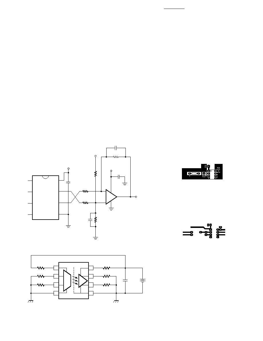
Figure 23. HCPL-7850 Block Diagram.
Figure 24. Recommended Application Circuit.
VOLTAGE
REGULATOR
CLOCK
GENERATOR
MODULATOR
ENCODER
LED DRIVE
CIRCUIT
DETECTOR
CIRCUIT
DECODER
AND D/A
FILTER
ISO-AMP
OUTPUT
VOLTAGE
REGULATOR
ISO-AMP
INPUT
ISOLATION
BOUNDARY
0.1 µF
+5 V
VOUT
8
7
6
1
3
U2
5
2
4
R1
2.00 K
+15 V
C8
0.1 µF
0.1 µF
-15 V
≠
+
MC34081
R3
10.0 K
HCPL-7850
C4
R4
10.0 K
C6
150 pF
U3
U1
78L05
IN OUT
C1
C2
0.01
µF
R5
68
GATE DRIVE
CIRCUIT
POSITIVE
FLOATING
SUPPLY
∑ ∑ ∑
HV+
∑ ∑ ∑
HV≠
∑ ∑ ∑
≠
+
RSENSE
MOTOR
C5
150 pF
0.1
µF
0.1
µF
C3
C7
R2
2.00 K
13
Applications Information
Functional Description
Figure 23 shows the primary
functional blocks of the HCPL-
7850. In operation, the sigma-
delta modulator converts the
analog input signal into a high-
speed serial bit stream. The time
average of this bit stream is
directly proportional to the input
signal. This stream of digital data
is encoded and optically
transmitted to the detector
circuit. The detected signal is
decoded and converted back into
an analog signal, which is filtered
to obtain the final output signal.
Figure 25. Single-Supply Post-Amplifier Circuit.
Figure 26. Top Layer of Printed
Circuit Board Layout.
Figure 27. Bottom Layer of a Printed
Circuit Board Layout.
Application Circuit
The recommended application
circuit is shown in Figure 24. A
floating power supply (which in
many applications could be the
same supply that is used to drive
the high-side power transistor) is
regulated to 5 V using a simple
three-terminal voltage regulator
(U1). The voltage from the
current sensing resistor, or shunt
(Rsense), is applied to the input
of the HCPL-7850 through an RC
anti-aliasing filter (R5, C3). And
finally, the differential output of
the isolation amplifier is
converted to a ground-referenced
single-ended output voltage with
a simple differential amplifier
circuit (U3 and associated
components). Although the
application circuit is relatively
simple, a few recommendations
should be followed to ensure
optimal performance.
Supplies and Bypassing
As mentioned above, an
inexpensive three-terminal
regulator can be used to reduce
the gate-drive power supply
voltage to 5 V. To help attenuate
high frequency power supply
noise or ripple, a resistor or
0.1 µF
+5 V
VOUT
8
7
6
1
3
U2
5
2
4
R1
10.0 K
+5 V
C8
0.1 µF
≠
+
MC34071
R3
10.0 K
HCPL-7850
C4
R4B
20.0 K
C6
150 pF
U3
R4A
20.0 K
+5 V
C5
150 pF
R2
10.0 K
C3
C2
C4
R5
TO R
SENSE+
TO R
SENSE≠
TO V
DD1
TO V
DD2
V
OUT+
V
OUT≠
Figure 28. Operating Circuit for Burn-In and Steady State Life Tests.
1
2
3
4
8
7
6
5
VDD
VIN+
VIN≠
GND
VDD
VOUT+
VOUT≠
GND
+
≠
+
≠
27
27
1 k
1 k
1 k
1 k
(+)
(≠)
VDD
5.5 VDC
0.1 µF
CONDITIONS: I
CC
=17.5mA
T
A
=+125∞C

14
inductor can be used in series
with the input of the regulator to
form a low-pass filter with the
regulator's input bypass
capacitor.
As shown in Figure 24, a 0.1
µ
F
bypass capacitor (C2, C4) should
be located as close as possible to
the input and output power
supply pins of the HCPL-7850.
The bypass capacitors are
required because of the high-
speed digital nature of the signals
inside the isolation amplifier. A
0.01
µ
F bypass capacitor (C3) is
also recommended at the input
pin(s) due to the switched-
capacitor nature of the input
circuit. The input bypass
capacitor should be at least
1000 pF to maintain gain
accuracy of the isolation
amplifier.
Inductive coupling between the
input power-supply capacitor and
the input circuit, including the
input bypass capacitor and the
input leads of the HCPL-7850,
can introduce additional DC
offset in the circuit. Several steps
can be taken to minimize the
mutual coupling between the two
parts of the circuit, thereby
improving the offset performance
of the design. Separate the two
bypass capacitors C2 and C3 as
much as possible (even putting
them on opposite sides of the PC
board), while keeping the total
lead lengths, including traces, of
each bypass capacitor less than
20 mm. PC board traces should
be made as short as possible and
placed close together or over
ground plane to minimize loop
area and pickup of stray magnetic
fields. Avoid using sockets, as
they will typically increase both
loop area and inductance. And
finally, using capacitors with
small body size and orienting
them perpendicular to each other
on the PC board can also help.
For more information concerning
this effect, see Application Note
1078, Designing with Agilent
Technologies Isolation
Amplifiers
.
Shunt Resistor Selections
The current-sensing shunt
resistor should have low
resistance (to minimize power
dissipation), low inductance (to
minimize di/dt induced voltage
spikes which could adversely
affect operation), and reasonable
tolerance (to maintain overall
circuit accuracy). The value of
the shunt should be chosen as a
compromise between minimizing
power dissipation by making the
shunt resistance smaller and
improving circuit accuracy by
making it larger and utilizing the
full input range of the HCPL-
7850. Agilent Technologies
recommends four different shunts
which can be used to sense
average currents in motor drives
up to 35 A and 35 hp. Table 1
shows the maximum current and
horsepower range for each of the
LVR-series shunts from Dale.
Even higher currents can be
sensed with lower value shunts
available from vendors such as
Dale, IRC, and Isotek
(Isabellenhuette). When sensing
currents large enough to cause
significant heating of the shunt,
the temperature coefficient of the
shunt can introduce nonlinearity
due to the signal dependent
temperature rise of the shunt.
Using a heat sink for the shunt or
using a shunt with a lower
tempco can help minimize this
effect. The Application Note
1078, Designing with Agilent
Technologies Isolation
Amplifiers
, contains additional
information on designing with
current shunts.
The recommended method for
connecting the isolation amplifier
to the shunt resistor is shown in
Figure 24. Pin 2 (V
IN+
) is
connected to the positive
terminal of the shunt resistor,
while pin 3 (V
IN≠
) is shorted to
pin 4 (GND1), with the power-
supply return path functioning as
the sense line to the negative
terminal of the current shunt.
This allows a single pair of wires
or PC board traces to connect the
isolation amplifier circuit to the
shunt resistor. In some
applications, however, supply
currents flowing through the
power-supply return path may
cause offset or noise problems. In
this case, better performance
may be obtained by connecting
pin 3 to the negative terminal of
the shunt resistor separate from
the power supply return path.
When connected this way, both
input pins should be bypassed.
Whether two or three wires are
used, it is recommended that
twisted-pair wire or very close PC
board traces be used to connect
the current shunt to the isolation
amplifier circuit to minimize
electromagnetic interference to
the sense signal.
The 68
resistor in series with
the input lead forms a low-pass
anti-aliasing filter with the input
bypass capacitor with a 200 kHz
bandwidth. The resistor
performs another important
function as well; it dampens any
ringing which might be present in
the circuit formed by the shunt,
the input bypass capacitor, and
the wires or traces connecting the
two. Undampened ringing of the
input circuit near the input
sampling frequency can alias into
the baseband producing what
might appear to be noise at the
output of the device. To be

15
effective, the damping resistor
should be at least 39
.
PC Board Layout
In addition to affecting offset, the
layout of the PC board can also
affect the common mode
rejection (CMR) performance of
the isolation amplifier, due
primarily to stray capacitive
coupling between the input and
the output circuits. To obtain
optimal CMR performance, the
layout of the printed circuit board
(PCB) should minimize any stray
coupling by maintaining the
maximum possible distance
between the input and output
sides of the circuit and ensuring
that any ground plane on the PCB
does not pass directly below the
HCPL-7850. Using surface mount
components can help achieve
many of the PCB objectives
discussed in the preceding
paragraphs. An example through-
hole PCB layout illustrating some
of the more important layout
recommendations is shown in
Figures 26 and 27. See
Applications Note 1078,
Designing with Agilent
Technologies Isolation
Amplifiers
, for more information
on PCB layout consideration.
Post-Amplifier Circuit
The recommended application
circuit (Figure 24) includes a
post-amplifier circuit that serves
three functions: to reference the
output signal to the desired level
(usually ground), to amplify the
signal to appropriate levels, and
to help filter output noise. The
particular op-amp used in the
post-amp is not critical; however,
it should have low enough offset
and high enough bandwidth and
slew rate so that it does not
adversely affect circuit
performance. The offset of the
op-amp should be low relative to
the output offset of the HCPL-
7850, or less than about 5 mV.
To maintain overall circuit
bandwidth, the post-amplifier
circuit should have a bandwidth
at least twice the minimum
bandwidth of the isolation
amplifier, or about 200 kHz. To
obtain a bandwidth of 200 kHz
with a gain of 5, the op-amp
should have a gain-bandwidth
greater than 1 mHz. The post-
amplifier circuit includes a pair of
capacitors (C5 and C6) that form
a single-pole low-pass filter.
These capacitors allow the
bandwidth of the post-amp to be
adjusted independently of the
gain and are useful for reducing
the output noise from the
isolation amplifier (doubling the
capacitor values halves the circuit
bandwidth). The component
values shown in Figure 24 form a
differential amplifier with a gain
of 5 and a cutoff frequency of
approximately 100 kHz, and were
chosen as a compromise between
low noise and fast response
times. The overall recommended
application circuit has a
bandwidth of 66 kHz, a rise time
of 5.2
µ
s and a delay to 90% of
8.5
µ
s.
The gain-setting resistors in the
post-amp should have a tolerance
of 1% or better to ensure
adequate CMRR and gain
tolerance for the overall circuit.
Resistor networks with even
better ratio tolerances can be
used which offer better
performance, as well as reducing
the total component count and
board space.
The post-amplifier circuit can be
easily modified to allow for
single-supply operation. Figure
25 shows a schematic for a post
amplifier for use in 5 V single
supply applications. One
additional resistor is needed and
the gain is decreased to 1 to
allow circuit operation over the
full input voltage range. See
Application Note 1078,
Designing with Agilent
Technologies Isolation
Amplifiers
, for more information
on the post-amplifier circuit.
Other Information
As mentioned above, reducing the
bandwidth of the post amplifier
circuit reduces the amount of
output noise. Figure 22 shows
how the output noise changes as
a function of the post-amplifier
bandwidth. The post-amplifier
circuit exhibits a first-order low-
pass filter characteristic. For the
same filter bandwidth, a higher-
order filter can achieve even
better attenuation of modulation
noise due to the second-order
noise shaping of the sigma-delta
modulator. For more information
on the noise characteristics of the
HCPL-7850, see Application Note
1078, Designing with Agilent
Technologies Isolation
Amplifiers
.
The HCPL-7850 can also be used
to isolate signals with amplitudes
larger than its recommended
input range through the use of a
resistive voltage divider at its
input. The only restrictions are
that the impedance of the divider
be relatively small (less than 1 K
so that the input resistance (480
K
) and input bias current (0.6
A) do not affect the accuracy of
the measurement. An input
bypass capacitor is still required,
although the 68
series damping
resistor is not. (The resistance of
the voltage divider provides the
same function.) The low pass
filter formed by the divider
resistance and the input bypass
capacitor may limit the
achievable bandwidth.
MIL-PRF-38534 Class H and
DSCC SMD Test Program
Agilent Technologies' Hi-Rel
Optocouplers are in compliance
with MIL-PRF-38534 Class H.
Class H devices are also in
compliance with DSCC drawing
5962-97557.
Testing consists of 100%
screening and quality
conformance inspection to
MIL-PRF-38534.
Table 1. Current Shunt Summary.
Maximum
Maximum
Maximum
Shunt
Power
Average
Horsepower
Shunt Resistor Part Number
Resistance
Dissipation
Current
Range
LVR-3.05-1%
50 m
3 W
3 A
0.8 to 3.0 hp
LVR-3.02-1%
20 m
3 W
8 A
2.2 to 8.0 hp
LVR-3.01-1%
10 m
3 W
15 A
4.1 to 15 hp
LVR-5.005-1%
5 m
5 W
35 A
9.6 to 35 hp
www.semiconductor.agilent.com
Data subject to change.
Copyright © 2000 Agilent Technologies
Osoletes 5966-2716E
5968-9405E (11/00)