 | –≠–ª–µ–∫—Ç—Ä–æ–Ω–Ω—ã–π –∫–æ–º–ø–æ–Ω–µ–Ω—Ç: HCPL-814 | –°–∫–∞—á–∞—Ç—å:  PDF PDF  ZIP ZIP |

Agilent HCPL-814
AC Input Phototransistor
Optocoupler
High Density Mounting Type
Data Sheet
Functional Diagram
CAUTION: It is advised that normal static precautions be taken in handling and assembly of this component to
prevent damage and/or degradation which may be induced by ESD.
Features
∑ AC input response
∑ High input-output isolation voltage
(V
iso
= 5,000 V
rms
)
∑ Low collector dark current
(I
CEO
: max. 10
-7
A at V
CE
= 20 V)
∑ Current transfer ratio
(CTR: min. 20% at I
F
=
±
1 mA,
V
CE
= 5 V)
∑ Response time
(t
r
: typ. 4
µ
s at V
CE
= 2 V, I
C
= 2 mA,
R
L
= 100
)
∑ Compact dual-in-line package
∑ UL approved
∑ CSA approved
∑ IEC/EN/DIN EN 60747-5-2
approved
∑ Options available:
≠ Leads with 0.4" (10.16 mm)
spacing (W00)
≠ Leads bend for surface
mounting (300)
≠ Tape and reel for SMD (500)
≠ IEC/EN/DIN EN 60747-5-2
approvals (060)
Applications
∑ Detecting or monitoring AC signals
∑ AC line/digital logic isolation
∑ Programmable logic controllers
∑ AC/DC ≠ input modules
Ordering Information
Specify Part Number followed by
Option Number (if desired).
HCPL-814-XXXE
Lead Free
Option Number
000 = No Options
060 = IEC/EN/DIN EN 60747-5-2
Option
W00 = 0.4" Lead Spacing Option
300 = Lead Bend SMD Option
500 = Tape and Reel Packaging
Option
00A = Rank Mark A
Description
The HCPL-814 contains a
phototransistor, optically coupled
to two light emitting diodes
connected inverse parallel. It can
operate directly by AC input
current. It is packaged in a 4-pin
DIP package and available in wide-
lead spacing option and lead bend
SMD option. Input-output isolation
voltage is 5000 V
rms
. Response
time, t
r
, is typically 4
µ
s and
minimum CTR is 20% at input
current of
±
1 mA.
4
1. ANODE, CATHODE
2. CATHODE, ANODE
3. EMITTER
4. COLLECTOR
3
1
2

2
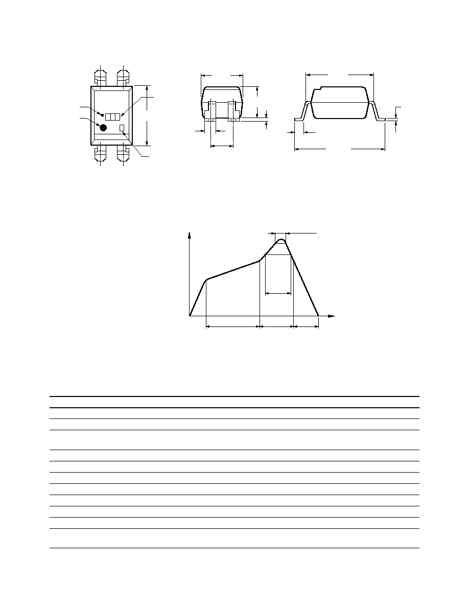
Package Outline Drawings
HCPL-814-000E
HCPL-814-W00E
HCPL-814-060E
6.5
±
0.5
(0.256)
DIMENSIONS IN MILLIMETERS AND (INCHES)
4.6
±
0.5
(0.181)
2.54
±
0.25
(0.1)
3.5
±
0.5
(0.138)
7.62
±
0.3
(0.3)
0.26
(0.010)
7.62 ~ 9.98
2.8
±
0.5
(0.110)
3.3
±
0.5
(0.130)
0.5
±
0.1
(0.02)
0.5
(0.02)
TYP.
DATE CODE *1
RANK *2
LEAD FREE
ANODE
A 814
Y W W
6.5
±
0.5
(0.256)
DIMENSIONS IN MILLIMETERS AND (INCHES)
4.6
±
0.5
(0.181)
2.54
±
0.25
(0.1)
3.5
±
0.5
(0.138)
7.62
±
0.3
(0.3)
0.26
(0.010)
7.62 ~ 9.98
2.8
±
0.5
(0.110)
3.3
±
0.5
(0.130)
0.5
±
0.1
(0.02)
0.5
(0.02)
TYP.
DATE CODE *1
RANK *2
LEAD FREE
ANODE
A 814 V
Y W W
6.5
±
0.5
(0.256)
DIMENSIONS IN MILLIMETERS AND (INCHES)
4.6
±
0.5
(0.181)
2.54
±
0.25
(0.1)
3.5
±
0.5
(0.138)
6.9
±
0.5
(0.272)
7.62
±
0.3
(0.3)
0.26
(0.010)
10.16
±
0.5
(0.4)
2.8
±
0.5
(0.110)
2.3
±
0.5
(0.09)
0.5
±
0.1
(0.02)
DATE CODE *1
RANK *2
LEAD FREE
ANODE
A 814
Y W W
3
HCPL-814-300E
Solder Reflow Temperature Profile
1) One-time soldering reflow is
recommended within the
condition of temperature and
time profile shown at right.
2) When using another soldering
method such as infrared ray
lamp, the temperature may rise
partially in the mold of the
device. Keep the temperature on
the package of the device within
the condition of (1) above.
30 seconds
60 ~ 150 sec
90 sec
60 sec
60 sec
25
∞
C
150
∞
C
200
∞
C
250
∞
C
260
∞
C (Peak Temperature)
217
∞
C
Time (sec)
Tem
perature (
∞
C)
Absolute Maximum Ratings
Parameters
Symbol
Min.
Max.
Units
Storage Temperature
T
S
≠55
125
∞C
Ambient Operating Temperature
T
A
≠30
100
∞C
Lead Solder Temperature for 10s
T
sol
260
∞C
(1.6 mm below seating plane)
Average Forward Current
I
F
±
50
mA
Input Power Dissipation
P
I
70
mW
Collector Current
I
C
50
mA
Collector-Emitter Voltage
V
CEO
35
V
Emitter-Collector Voltage
V
ECO
6
V
Collector Power Dissipation
P
C
150
mW
Total Power Dissipation
P
tot
200
mW
Isolation Voltage
V
iso
5000
V
rms
(AC for 1 minute, R.H. = 40 ~ 60%)
[1]
6.5
±
0.5
(0.256)
DIMENSIONS IN MILLIMETERS AND (INCHES)
4.6
±
0.5
(0.181)
2.54
±
0.25
(0.1)
3.5
±
0.5
(0.138)
7.62
±
0.3
(0.3)
0.26
(0.010)
10.16
±
0.3
(0.4)
1.2
±
0.1
(0.047)
0.35
±
0.25
(0.014)
1.0
±
0.25
(0.039)
A 814
Y W W
DATE CODE *1
RANK *2
LEAD FREE
ANODE

4
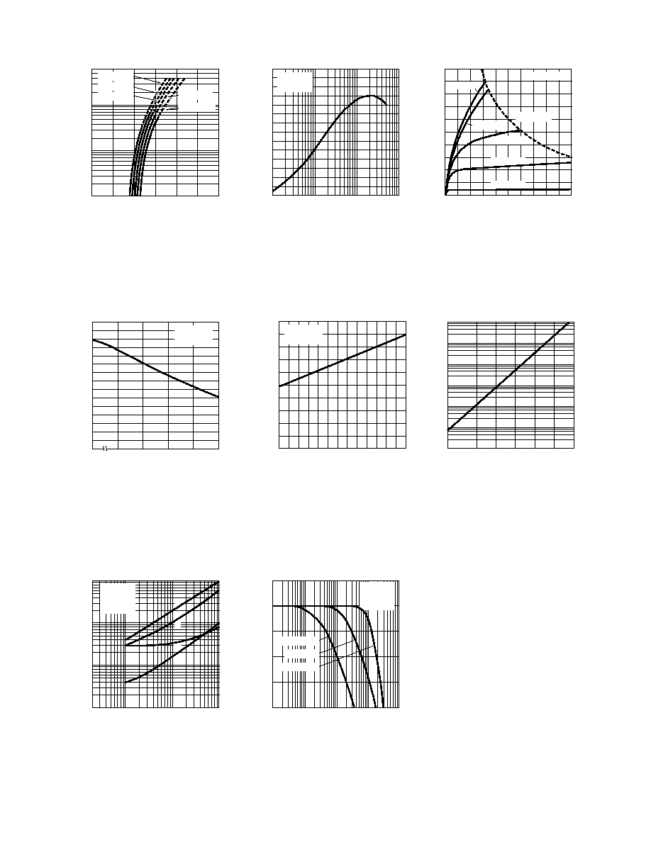
Figure 1. Forward current vs. temperature.
Figure 2. Collector power dissipation vs.
temperature.
Figure 3. Collector-emitter saturation voltage
vs. forward current.
Rank Mark
CTR (%)
Conditions
A
50 ~ 150
I
F
=
±
1 mA,
No Mark
20 ~ 300
V
CE
= 5 V,
T
A
= 25∞C
Notes:
1. Isolation voltage shall be measured using the following method:
(a) Short between anode and cathode on the primary side and between collector and emitter
on the secondary side.
(b) The isolation voltage tester with zero-cross circuit shall be used.
(c) The waveform of applied voltage shall be a sine wave.
2.
CTR = x 100%
I
C
I
F
Electrical Specifications (T
A
= 25∞C)
Parameter
Symbol
Min.
Typ.
Max.
Units
Test Conditions
Forward Voltage
V
F
≠
1.2
1.4
V
I
F
=
±
20 mA
Terminal Capacitance
C
t
≠
50
250
pF
V = 0, f = 1 kHz
Collector Dark Current
I
CEO
≠
≠
100
nA
V
CE
= 20 V, I
F
= 0
Collector-Emitter Breakdown Voltage
BV
CEO
35
≠
≠
V
I
C
= 0.1 mA, I
F
= 0
Emitter-Collector Breakdown Voltage
BV
ECO
6
≠
≠
V
I
E
= 10
µ
A, I
F
= 0
Collector Current
I
C
0.2
≠
3
mA
I
F
=
±
1 mA,
Current Transfer Ratio
[2]
CTR
20
≠
300
%
V
CE
= 5 V
Collector-Emitter Saturation Voltage
V
CE(sat)
≠
0.1
0.2
V
I
F
=
±
20 mA, I
C
= 1 mA
Isolation Resistance
R
iso
5 x 10
10
1 x 10
11
≠
DC 500 V
40 ~ 60% R.H.
Floating Capacitance
C
f
≠
0.6
1
pF
V = 0, f = 1 MHz
Cut-off Frequency
f
c
15
80
≠
kHz
V
CE
= 5 V, I
C
= 2 mA
R
L
= 100
, ≠3 dB
Response Time (Rise)
t
r
≠
4
18
µ
s
V
CE
= 2 V, I
C
= 2 mA,
Response Time (Fall)
t
f
≠
3
18
µ
s
R
L
= 100
0
IF ≠ FORWARD CURRENT ≠ mA
10.0
15.0
2
5.0
0
1
3
4
5
6
V
CE(SAT.)
≠ COLLECTOR-EMITTER
SATURATION VOLTAGE ≠ V
TA = 25∞C
IC = 0.5 mA
IC = 1 mA
IC = 3 mA
IC = 5 mA
IC = 7 mA
2.5
7.5
12.5
I F
≠
FORWARD CURRENT
≠
mA
0
TA ≠ AMBIENT TEMPERATURE ≠ ∞C
75
125
50
25
10
40
0
50
100
-30
60
30
20
P
C
≠
COLLECTOR POWER DISSIPATION
≠
mW
0
TA ≠ AMBIENT TEMPERATURE ≠ ∞C
100
50
200
150
75
125
25
0
50
100
-30
5
I F
≠
FORWARD CURRENT
≠
mA
1
VF ≠ FORWARD VOLTAGE ≠ V
2.0
3.0
10
5
500
1.0
0
TA = 75∞C
0.5
1.5
2.5
2
20
50
100
200
TA = 50∞C
TA = 25∞C
TA = 0∞C
TA = -25∞C
Figure 4. Forward current vs. forward voltage.
Figure 5. Current transfer ratio vs. forward
current.
Figure 6. Collector current vs. collector-
emitter voltage.
Figure 7. Relative current transfer ratio vs.
temperature.
Figure 8. Collector-emitter saturation
voltage vs. temperature.
Figure 9. Collector dark current vs.
temperature.
0
IF ≠ FORWARD CURRENT ≠ mA
10
100
40
0.2
0.1
20
60
120
140
CTR
≠
CURRENT TRANSFER RATIO
≠
%
80
100
0.5
20
1
50
5
2
VCE = 5 V
TA = 25∞C
I C
≠
COLLECTOR CURRENT
≠
mA
0
VCE ≠ COLLECTOR-EMITTER VOLTAGE ≠ V
6
10
40
20
50
3
0
PC (MAX.)
TA = 25∞C
I
F
= 30 mA
I
F
= 20 mA
I
F
= 5 mA
30
10
1
2
4
5
7
8
9
I
F
= 1 mA
I
F
= 10 mA
V
CE(SAT.)
≠
COLLECTOR-EMITTER
SATURATION VOLTAGE
≠
V
0
0.10
0.02
IC = 1 mA
IF = 20 mA
TA ≠ AMBIENT TEMPERATURE ≠ ∞C
80
40
-30
60
100
0.04
0.06
0.08
20
0
I CEO
≠
COLLECTOR DARK CURRENT
≠
A
TA ≠ AMBIENT TEMPERATURE ≠ ∞C
10
-12
10
-11
10
-10
10
-9
10
-8
10
-7
80
40
0
60
100
-30
10
-6
20
RELATIVE CURRENT TRANSFER RATIO
≠
%
0
100
50
150
VCE = 5 V
IF = 5 mA
TA ≠ AMBIENT TEMPERATURE ≠ ∞C
75
25
0
50
100
-30
Figure 10. Response time vs. load resistance.
Figure 11. Frequency response.
RESPONSE TIME
≠
µs
0.1
RL ≠ LOAD RESISTANCE ≠ k
0.1
5
1
0.5
0.2
0.5
0.2
2
10
2
1
5
10
20
50
100
VCE = 2 V
IC = 2 mA
TA = 25∞C
tf
tr
ts
td
VOLTAGE GAIN AV
≠
dB
f ≠ FREQUENCY ≠ kHz
0.5
10
2
-20
-10
1
5
0.2
0
100
RL = 10 k
RL = 1 k
RL = 100
1000
VCE = 2 V
IC = 2 mA
TA = 25∞C