Agilent HCPL-817
Phototransistor Optocoupler
High Density Mounting Type
Data Sheet
Features
∑ Current Transfer Ratio
(CTR: min. 50% at I
F
= 5 mA,
V
CE
= 5 V)
∑ High input-output isolation voltage
(V
iso
= 5000 Vrms)
∑ Response time (t
r
: typ., 4
µ
s at
V
CE
= 2 V, I
C
= 2 mA, R
L
= 100
)
∑ Compact dual-in-line package
∑ UL approved
∑ CSA approved
∑ VDE approved
∑ Options available:
≠ Leads with 0.4" (10.16 mm)
spacing (W00)
≠ Leads bends for surface
mounting (300)
≠ Tape and reel for SMD (500)
≠ VDE 0884 approvals (060)
Applications
∑ Signal transmission between
circuits of different potentials and
impedances
∑ I/O interfaces for computers
∑ Feedback circuit in power supply
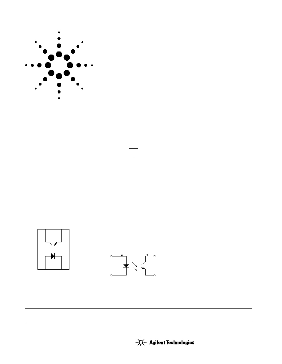
Description
The HCPL-817 contains a light
emitting diode optically coupled to
a phototransistor. It is packaged in
a 4-pin DIP package and available
in wide-lead spacing option and
lead bend SMD option. Input-output
isolation voltage is 5000 Vrms.
Response time, t
r
, is typically 4
µ
s
and minimum CTR is 50% at input
current of 5 mA.
Functional Diagram
Ordering Information
Specify part number followed by
Option Number (if desired).
HCPL-817-XXX
Option Number
060 = VDE0884 Option
W00 = 0.4" Lead Spacing Option
300 = Lead Bend SMD Option
500 = Tape and Reel Packaging
Option
00A = Rank Mark A
00B = Rank Mark B
00C = Rank Mark C
00D = Rank Mark D
00L = Rank Mark L
Schematic
4
3
1
2
PIN NO. AND INTERNAL
CONNECTION DIAGRAM
1. ANODE
2. CATHODE
3. EMITTER
4. COLLECTOR
1
2
ANODE
CATHODE
VF
+
≠
IF
4
3
COLLECTOR
EMITTER
IC
CAUTION: It is advised that normal static precautions be taken in handling and assembly of this component to
prevent damage and/or degradation which may be induced by ESD.

2
Package Outline Drawings
Package Outline ≠ Option W00
Package Outline ≠ Option 300
1
2
3
4
TYPE NUMBER
OPTION CODE
FOR OPTION 060
ONLY
PIN ONE DOT
A 817 V
YWW
6.5 ± 0.5
(0.256)
DIMENSIONS IN MILLIMETERS AND (INCHES)
4.6 ± 0.5
(0.181)
2.8 ± 0.5
(0.110)
2.54 ± 0.25
(0.1)
0.5 ± 0.1
(0.02)
3.5 ± 0.5
(0.138)
3.3 ± 0.5
(0.130)
0.5
(0.02)
7.62 ± 0.3
(0.3)
0.35 +0.15/-0.10
(0.014)
7.62 ~ 9.98
TYP.
RANK MARK
DATE CODE
6.5 ± 0.5
(0.256)
DIMENSIONS IN MILLIMETERS AND (INCHES)
4.6 ± 0.5
(0.181)
2.8 ± 0.5
(0.110)
2.54 ± 0.25
(0.1)
0.5 ± 0.1
(0.02)
3.5 ± 0.5
(0.138)
7.62 ± 0.3
(0.3)
0.35 +0.15/-0.10
(0.014)
10.16 ± 0.5
(0.4)
2.3 ± 0.5
(0.09)
6.9 ± 0.5
(0.272)
6.5 ± 0.5
(0.256)
DIMENSIONS IN MILLIMETERS AND (INCHES)
4.6 ± 0.5
(0.181)
2.54 ± 0.25
(0.1)
3.5 ± 0.5
(0.138)
7.62 ± 0.3
(0.3)
0.35 ± 0.25
(0.014)
10.16 ± 0.3
(0.4)
1.2 ± 0.1
(0.047)
0.35 ± 0.25
(0.014)
1.0 ± 0.25
(0.039)

3
Absolute Maximum Ratings (T
A
= 25∞C)
Storage Temperature, T
S
≠55∞C to +125∞C
Operating Temperature, T
A
≠30∞C to +100∞C
Lead Solder Temperature, max.
260∞C for 10 s
(1.6 mm below seating plane)
Average Forward Current, I
F
50 mA
Reverse Input Voltage, V
R
6 V
Input Power Dissipation, P
I
70 mW
Collector Current, I
C
50 mA
Collector-Emitter Voltage, V
CEO
35 V
Emitter-Collector Voltage, V
ECO
6 V
Collector Power Dissipation
150 mW
Total Power Dissipation
200 mW
Isolation Voltage, V
iso
(AC for 1 minute, R.H. = 40 ~ 60%)
5000 Vrms
* CTR = x 100%
I
C
I
F
Rank Mark
CTR (%)
Conditions
L
50 ~ 100
I
F
= 5 mA, V
CE
= 5 V, T
A
= 25
∞
C
A
80 ~ 160
B
130 ~ 260
C
200 ~ 400
D
300 ~ 600
Electrical Specifications (T
A
= 25∞C)
Parameter
Symbol
Min.
Typ.
Max.
Units
Test Conditions
Forward Voltage
V
F
≠
1.2
1.4
V
I
F
= 20 mA
Reverse Current
I
R
≠
≠
10
µ
A
V
R
= 4 V
Terminal Capacitance
C
t
≠
30
250
pF
V = 0, f = 1 KHz
Collector Dark Current
I
CEO
≠
≠
100
nA
V
CE
= 20 V
Collector-Emitter Breakdown Voltage
BV
CEO
35
≠
≠
V
I
C
= 0.1 mA
Emitter-Collector Breakdown Voltage
BV
ECO
6
≠
≠
V
I
E
= 10
µ
A
Collector Current
I
C
2.5
≠
30
mA
I
F
= 5 mA, V
CE
= 5 V,
*Current Transfer Ratio
CTR
50
≠
600
%
R
BE
=
Collector-Emitter Saturation Voltage
V
CE(sat)
≠
0.1
0.2
V
I
F
= 20 mA, I
C
= 1 mA
Response Time (Rise)
t
r
≠
4
18
µ
s
V
CC
= 2 V, I
C
= 2 mA
Response Time (Fall)
t
f
≠
3
18
µ
s
R
L
= 100
Cut-off Frequency
f
c
≠
80
≠
KHz
V
CC
= 5 V, I
C
= 2 mA
R
L
= 100
, ≠3 dB
Isolation Resistance
R
iso
5 x 10
10
1 x 10
11
≠
DC 500 V
40 ~ 60% R.H.
Floating Capacitance
C
f
≠
0.6
1.0
pF
V = 0, f = 1 MHz
4
Figure 1. Forward current vs. temperature.
Figure 2. Collector power dissipation vs.
temperature.
Figure 3. Collector-emitter saturation voltage
vs. forward current.
I F
≠ FORWARD CURRENT ≠ mA
0
TA ≠ AMBIENT TEMPERATURE ≠ ∞C
75
125
50
25
10
40
0
50
100
-30
60
30
20
P
C
≠ COLLECTOR POWER DISSIPATION ≠ mW
0
TA ≠ AMBIENT TEMPERATURE ≠ ∞C
100
50
200
150
75
125
25
0
50
100
-30
0
IF ≠ FORWARD CURRENT ≠ mA
14
20
2
6
0
1
3
4
5
6
V
CE(SAT.)
≠ COLLECTOR-EMITTER
SATURATION VOLTAGE ≠ V
TA = 25∞C
IC = 0.5 mA
IC = 1 mA
IC = 3 mA
IC = 6 mA
IC = 7 mA
2
4
8
10 12
16 18
Figure 4. Forward current vs. forward voltage.
Figure 5. Current transfer ratio vs. forward
current.
Figure 6. Collector current vs. collector-
emitter voltage.
Figure 7. Relative current transfer ratio vs.
temperature.
Figure 8. Collector-emitter saturation
voltage vs. temperature.
Figure 9. Collector dark current vs.
temperature.
I C
≠ COLLECTOR CURRENT ≠ mA
0
VCE ≠ COLLECTOR-EMITTER VOLTAGE ≠ V
6
9
40
20
50
3
0
PC (MAX.)
TA = 25∞C
IF = 30 mA
IF = 20 mA
IF = 10 mA
IF = 5 mA
30
10
IF = 20 mA
IF = 10 mA
1
2
4
5
7
8
RELATIVE CURRENT TRANSFER RATIO ≠ %
0
100
50
150
VCE = 5 V
IF = 5 mA
TA ≠ AMBIENT TEMPERATURE ≠ ∞C
75
25
0
50
100
-30
V
CE(SAT.)
≠ COLLECTOR-EMITTER
SATURATION VOLTAGE ≠ V
0
0.10
0.02
0.16
IC = 1 mA
IF = 20 mA
TA ≠ AMBIENT TEMPERATURE ≠ ∞C
75
25
0
50
100
-25
0.04
0.06
0.08
0.12
0.14
I CEO
≠ COLLECTOR DARK CURRENT ≠ A
TA ≠ AMBIENT TEMPERATURE ≠ ∞C
VCE = 20 V
10
-11
10
-10
10
-9
10
-8
10
-7
10
-6
75
25
0
50
100
-25
10
-5
I F
≠ FORWARD CURRENT ≠ mA
1
VF ≠ FORWARD VOLTAGE ≠ V
2.0
3.0
10
5
500
1.0
0
TA = 75∞C
0.5
1.5
2.5
2
20
50
100
200
TA = 50∞C
TA = 25∞C
TA = 0∞C
TA = -25∞C
0
IF ≠ FORWARD CURRENT ≠ mA
10
50
40
200
2
1
20
60
120
140
160
CTR ≠ CURRENT TRANSFER RATIO ≠ %
VCE = 5 V
TA = 25∞C
80
100
180
5
20

5
Figure 10. Response time vs. load resistance.
Figure 11. Frequency response.
RESPONSE TIME ≠ µs
0.1
RL ≠ LOAD RESISTANCE ≠ k
0.1
5
1
0.5
0.2
0.5
500
0.2
2
10
0.05
2
VCE = 2 V
IC = 2 mA
TA = 25∞C
tf
tr
1
5
10
20
50
100
200
ts
td
VOLTAGE GAIN AV ≠ dB
f ≠ FREQUENCY ≠ kHz
1
20
500
5
20
10
2
10
50
0.5
0
100 200
RL = 10 k
RL = 1 k
RL = 100
VCE = 2 V
IC = 2 mA
TA = 25∞C
Test Circuit for Response Time
Test Circuit for Frequency Response
VCC
RD
RL
OUTPUT
~
VCC
RD
INPUT
RL
OUTPUT
INPUT
OUTPUT
10%
90%
td
tr
tf
ts