 | –≠–ª–µ–∫—Ç—Ä–æ–Ω–Ω—ã–π –∫–æ–º–ø–æ–Ω–µ–Ω—Ç: HCPL-J312 | –°–∫–∞—á–∞—Ç—å:  PDF PDF  ZIP ZIP |

2.0 Amp Output Current IGBT
Gate Drive Optocoupler
Technical Data
HCPL-3120
HCPL-J312
HCNW3120
Features
∑ 2.0 A Minimum Peak Output
Current
∑ 15 kV/
µ
s Minimum Common
Mode Rejection (CMR) at
V
CM
= 1500 V
∑ 0.5 V Maximum Low Level
Output Voltage (V
OL
)
Eliminates Need for Negative
Gate Drive
∑ I
CC
= 5 mA Maximum Supply
Current
∑ Under Voltage Lock-Out
Protection (UVLO) with
Hysteresis
∑ Wide Operating V
CC
Range:
15 to 30 Volts
∑ 500 ns Maximum Switching
Speeds
∑ Industrial Temperature
Range: -40
∞
C to 100
∞
C
∑ Safety Approval
UL Recognized
2500 Vrms for 1 min. for
HCPL-3120
3750 Vrms for 1 min. for
HCPL-J312
5000 Vrms for 1 min. for
HCNW3120
CSA Approval
VDE 0884 Approved
V
IORM
= 630 Vpeak for
HCPL-3120 (Option 060)
V
IORM
= 891 Vpeak for
HCPL-J312
V
IORM
= 1414 Vpeak for
HCNW3120
BSI Certified (HCNW3120
only) (Pending)
Applications
∑ IGBT/MOSFET Gate Drive
∑ AC/Brushless DC Motor
Drives
∑ Industrial Inverters
∑ Switch Mode Power
Supplies
A 0.1
µ
F bypass capacitor must be connected between pins 5 and 8.
CAUTION: It is advised that normal static precautions be taken in handling and assembly of this component
to prevent damage and/or degradation which may be induced by ESD.
Functional Diagram
TRUTH TABLE
V
CC
- V
EE
V
CC
- V
EE
"POSITIVE GOING" "NEGATIVE GOING"
LED
(i.e., TURN-ON)
(i.e., TURN-OFF)
V
O
OFF
0 - 30 V
0 - 30 V
LOW
ON
0 - 11 V
0 - 9.5 V
LOW
ON
11 - 13.5 V
9.5 - 12 V
TRANSITION
ON
13.5 - 30 V
12 - 30 V
HIGH
1
3
SHIELD
2
4
8
6
7
5
N/C
CATHODE
ANODE
N/C
VCC
VO
VO
VEE
1
3
SHIELD
2
4
8
6
7
5
N/C
CATHODE
ANODE
N/C
VCC
N/C
VO
VEE
HCNW3120
HCPL-3120/J312

2
Description
The HCPL-3120 contains a
GaAsP LED while the HCPL-J312
and the HCNW3120 contain an
AlGaAs LED. The LED is optically
coupled to an integrated circuit
with a power output stage. These
optocouplers are ideally suited
for driving power IGBTs and
MOSFETs used in motor control
inverter applications. The high
operating voltage range of the
output stage provides the drive
voltages required by gate
controlled devices. The voltage
and current supplied by these
optocouplers make them ideally
suited for directly driving IGBTs
with ratings up to 1200 V/100 A.
For IGBTs with higher ratings,
the HCPL-3120 series can be
used to drive a discrete power
stage which drives the IGBT gate.
The HCNW3120 has the highest
insulation voltage of
V
IORM
= 1414 Vpeak in the
VDE0884. The HCPL-J312 has an
insulation voltage of
V
IORM
= 891 Vpeak and the
V
IORM
= 630 Vpeak is also
available with the HCPL-3120
(Option 060).
Selection Guide
Part Number
HCPL-3120
HCPL-J312
HCNW3120
HCPL-3150*
Output Peak Current ( I
O
)
2.0 A
2.0 A
2.0 A
0.5 A
VDE0884 Approval
V
IORM
= 630 Vpeak
V
IORM
= 891 Vpeak
V
IORM
= 1414 Vpeak
V
IORM
= 630 Vpeak
(Option 060)
(Option 060)
*The HCPL-3150 Data sheet available. Contact Agilent sales representative or authorized distributor.
Ordering Information
Specify Part Number followed by Option Number (if desired)
Example:
HCPL-3120#XXX
060 = VDE0884, V
IORM
= 630 Vpeak (HCPL-3120 only)
300 = Gull Wing Surface Mount Option
500 = Tape and Reel Packaging Option
Option 500 contains 1000 units (HCPL-3120/J312), 750 units (HCNW3120) per reel.
Other options contain 50 units (HCPL-3120/J312), 42 units (HCNW312) per tube.
Option data sheets available. Contact Agilent sales representative or authorized distributor.

3
0.635 ± 0.25
(0.025 ± 0.010)
12∞ NOM.
9.65 ± 0.25
(0.380 ± 0.010)
0.635 ± 0.130
(0.025 ± 0.005)
7.62 ± 0.25
(0.300 ± 0.010)
5
6
7
8
4
3
2
1
9.65 ± 0.25
(0.380 ± 0.010)
6.350 ± 0.25
(0.250 ± 0.010)
1.016 (0.040)
1.194 (0.047)
1.194 (0.047)
1.778 (0.070)
9.398 (0.370)
9.906 (0.390)
4.826
(0.190)
TYP.
0.381 (0.015)
0.635 (0.025)
PAD LOCATION (FOR REFERENCE ONLY)
1.080 ± 0.320
(0.043 ± 0.013)
4.19
(0.165)
MAX.
1.780
(0.070)
MAX.
1.19
(0.047)
MAX.
2.54
(0.100)
BSC
DIMENSIONS IN MILLIMETERS (INCHES).
LEAD COPLANARITY = 0.10 mm (0.004 INCHES).
0.254
+ 0.076
- 0.051
(0.010
+ 0.003)
- 0.002)
Package Outline Drawings
HCPL-3120 and HCPL-J312 Outline Drawing (Standard DIP Package)
HCPL-3120 and HCPL-J312 Gull Wing Surface Mount Option 300 Outline Drawing
9.65 ± 0.25
(0.380 ± 0.010)
1.78 (0.070) MAX.
1.19 (0.047) MAX.
A XXXXZ
YYWW
DATE CODE
1.080 ± 0.320
(0.043 ± 0.013)
2.54 ± 0.25
(0.100 ± 0.010)
0.51 (0.020) MIN.
0.65 (0.025) MAX.
4.70 (0.185) MAX.
2.92 (0.115) MIN.
DIMENSIONS IN MILLIMETERS AND (INCHES).
5
6
7
8
4
3
2
1
5∞ TYP.
OPTION CODE*
0.254
+ 0.076
- 0.051
(0.010
+ 0.003)
- 0.002)
7.62 ± 0.25
(0.300 ± 0.010)
6.35 ± 0.25
(0.250 ± 0.010)
TYPE NUMBER
* MARKING CODE LETTER FOR OPTION NUMBERS.
"V" = OPTION 060
OPTION NUMBERS 300 AND 500 NOT MARKED.

4
1.00 ± 0.15
(0.039 ± 0.006)
7∞ NOM.
12.30 ± 0.30
(0.484 ± 0.012)
0.75 ± 0.25
(0.030 ± 0.010)
11.00
(0.433)
5
6
7
8
4
3
2
1
11.15 ± 0.15
(0.442 ± 0.006)
9.00 ± 0.15
(0.354 ± 0.006)
1.3
(0.051)
12.30 ± 0.30
(0.484 ± 0.012)
6.15
(0.242)TYP.
0.9
(0.035)
PAD LOCATION (FOR REFERENCE ONLY)
1.78 ± 0.15
(0.070 ± 0.006)
4.00
(0.158)
MAX.
1.55
(0.061)
MAX.
2.54
(0.100)
BSC
DIMENSIONS IN MILLIMETERS (INCHES).
LEAD COPLANARITY = 0.10 mm (0.004 INCHES).
0.254
+ 0.076
- 0.0051
(0.010
+ 0.003)
- 0.002)
MAX.
HCNW3120 Outline Drawing (8-Pin Wide Body Package)
HCNW3120 Gull Wing Surface Mount Option 300 Outline Drawing
5
6
7
8
4
3
2
1
11.15 ± 0.15
(0.442 ± 0.006)
1.78 ± 0.15
(0.070 ± 0.006)
5.10
(0.201)
MAX.
1.55
(0.061)
MAX.
2.54 (0.100)
TYP.
DIMENSIONS IN MILLIMETERS (INCHES).
7∞ TYP.
0.254
+ 0.076
- 0.0051
(0.010
+ 0.003)
- 0.002)
11.00
(0.433)
9.00 ± 0.15
(0.354 ± 0.006)
MAX.
10.16 (0.400)
TYP.
A
HCNWXXXX
YYWW
DATE CODE
TYPE NUMBER
0.51 (0.021) MIN.
0.40 (0.016)
0.56 (0.022)
3.10 (0.122)
3.90 (0.154)

5
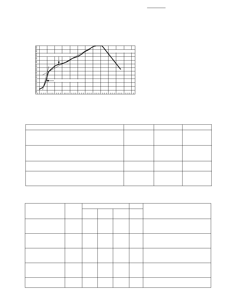
Reflow Temperature Profile
Regulatory Information
Agency/Standard
HCPL-3120
HCPL-J312
HCNW3120
Underwriters Laboratory (UL)
Recognized under UL 1577, Component Recognition
Program, Category, File E55361
Canadian Standards Association (CSA)
File CA88324, per Component Acceptance
Notice #5
Verband Deutscher Electrotechniker (VDE)
DIN VDE 0884 (June 1992)
Option 060
British Standards Institute (BSI)
Pending
Certification According to BS EN60065: 1994
(BS415:1994), BS EN60950: 1992 (BS7002:1992)
240
T = 115∞C, 0.3∞C/SEC
0
T = 100∞C, 1.5∞C/SEC
T = 145∞C, 1∞C/SEC
TIME ≠ MINUTES
TEMPERATURE ≠ ∞C
220
200
180
160
140
120
100
80
60
40
20
0
260
1
2
3
4
5
6
7
8
9
10
11
12
MAXIMUM SOLDER REFLOW THERMAL PROFILE
(NOTE: USE OF NON-CHLORINE ACTIVATED FLUXES IS RECOMMENDED.)
Insulation and Safety Related Specifications
Value
HCPL- HCPL-
HCNW
Parameter
Symbol
3120
J312
3120
Units
Conditions
Minimum External
L(101)
7.1
7.4
9.6
mm
Measured from input terminals to
Air Gap (Clearance)
output terminals, shortest distance
through air.
Minimum External
L(102)
7.4
8.0
10.0
mm
Measured from input terminals to
Tracking (Creepage)
output terminals, shortest distance
path along body.
Minimum Internal
0.08
0.5
1.0
mm
Insulation thickness between emitter
Plastic Gap
and detector; also known as distance
(Internal Clearance)
through insulation.
Tracking Resistance
CTI
>175
>175
>200
Volts
DIN IEC 112/VDE 0303 Part 1
(Comparative
Tracking Index)
Isolation Group
IIIa
IIIa
IIIa
Material Group (DIN VDE 0110, 1/89,
Table 1)


