 | –≠–ª–µ–∫—Ç—Ä–æ–Ω–Ω—ã–π –∫–æ–º–ø–æ–Ω–µ–Ω—Ç: HCPL-M700 | –°–∫–∞—á–∞—Ç—å:  PDF PDF  ZIP ZIP |
CAUTION: The small device geometries inherent to the design of this bipolar component increase the component's
susceptibility to damage from electrostatic discharge (ESD). It is advised that normal static precautions be taken
in handling and assembly of this component to prevent damage and/or degradation which may be induced by
ESD.
Small Outline, 5 Lead, Low
Input Current, High Gain
Optocouplers
Technical Data
HCPL-M700
HCPL-M701
Description
These small outline, low input
current, high gain optocouplers
are single channel devices in a
five lead miniature footprint. They
are electrically equivalent to the
following Agilent optocouplers:
Features
∑ Surface Mountable
∑ Very Small, Low Profile
JEDEC Registered
Package Outline
∑ Compatible with Infrared
Vapor Phase Reflow and
Wave Soldering Processes
∑ High Current Transfer
Ratio - 2000%
∑ Low Input Current
Capability - 0.5 mA
∑ TTL Compatible Output -
V
OL
= 0.1 V
∑ Guaranteed ac and dc
Performance Over
Temperature: 0
∞
C to 70
∞
C
∑ High Output Current -
60 mA
∑ Recognized under the
Component Program of
U.L. (File No. E55361) for
Dielectric Withstand Proof
Test Voltage of 3750 Vac, 1
Minute
∑ Lead Free Option "-000E"
The SO-5 JEDEC registered (MO-
155) package outline does not
require "through holes" in a PCB.
This package occupies
approximately one-fourth the
footprint area of the standard
dual-in-line package. The lead
profile is designed to be com-
patible with standard surface
mount processes.
These high gain series opto-
couplers use a Light Emitting
Diode and an integrated high gain
photodetector to provide
extremely high current transfer
ratio between input and output.
Separate pins for the photodiode
and output stage results in TTL
compatible saturation voltages
and high speed operation. Where
desired the V
CC
and V
O
terminals
may be tied together to achieve
conventional photodarlington
operation.
SO-5 Package
Standard DIP
SO-8 Package
HCPL-M700
6N138
HCPL-0700
HCPL-M701
6N139
HCPL-0701

2
The HCPL-M701 is for use in
CMOS, LSTTL or other low power
applications. A 400% minimum
current transfer ratio is
guaranteed over a 0-70
∞
C
operating range for only 0.5 mA
of LED current.
The HCPL-M700 is designed for
use mainly in TTL applications.
Current Transfer Ratio is 300%
minimum over 0-70
∞
C for an LED
current of 1.6 mA [1 TTL Unit
Load (U.L.)]. A 300% CTR
enables operation with 1 U.L. out
with a 2.2 k
pull-up resistor.
Selection for lower input currents
down to 250
µ
A is available upon
request.
Outline Drawing (JEDEC MO-155)
Applications
∑ Ground Isolate Most Logic
Families - TTL/TTL, CMOS/
TTL, CMOS/CMOS, LSTTL/
TTL, CMOS/LSTTL
∑ Low Input Current Line
Receiver
∑ EIA RS232C Line Receiver
∑ Telephone Ring Detector
∑ ac Line Voltage Status
Indicator - Low Input
Power Dissipation
∑ Low Power Systems -
Ground Isolation
Schematic
Land Pattern Recommendation
IF
6
VCC
1
3
ICC
VF
ANODE
CATHODE
+
≠
5
4
GND
VO
IO
MXXX
XXX
6
5
4
3
1
7.0 ± 0.2
(0.276 ± 0.008)
2.5 ± 0.1
(0.098 ± 0.004)
0.102 ± 0.102
(0.004 ± 0.004)
V
CC
V
OUT
GND
CATHODE
ANODE
4.4 ± 0.1
(0.173 ± 0.004)
1.27
(0.050)
BSC
0.15 ± 0.025
(0.006 ± 0.001)
0.71
(0.028)
MIN.
0.4 ± 0.05
(0.016 ± 0.002)
3.6 ± 0.1*
(0.142 ± 0.004)
DIMENSIONS IN MILLIMETERS (INCHES)
* MAXIMUM MOLD FLASH ON EACH SIDE IS 0.15 mm (0.006)
NOTE: FLOATING LEAD PROTRUSION IS 0.15 mm (6 mils) MAX.
7∞ MAX.
MAX. LEAD COPLANARITY
= 0.102 (0.004)
8.27
(0.325)
2.0
(0.080)
2.5
(0.10)
1.3
(0.05)
0.64
(0.025)
4.4
(0.17)
3
Absolute Maximum Ratings
(No Derating Required up to 85
∞
C)
Storage Temperature ................................................. -55
∞
C to +125
∞
C
Operating Temperature ............................................... -40
∞
C to +85
∞
C
Average Input Current - I
F
........................................................ 20 mA
Peak Input Current - I
F
.............................................................. 40 mA
(50% duty cycle, 1 ms pulse width)
Peak Transient Input Current - I
F
.............................................. 1.0 A
(
1
µ
s pulse width, 300 pps)
Reverse Input Voltage - V
R
.............................................................. 5 V
Input Power Dissipation ........................................................... 35 mW
Output Current - I
O
(Pin 5) ........................................................ 60 mA
Supply and Output Voltage - V
CC
(Pin 6-4),V
O
(Pin 5-4)
HCPL-M700 ................................................................... -0.5 V to 7 V
HCPL-M701 ................................................................. -0.5 V to 18 V
Output Power Dissipation ....................................................... 100 mW
Infrared and Vapor Phase Reflow Temperature .................. see below
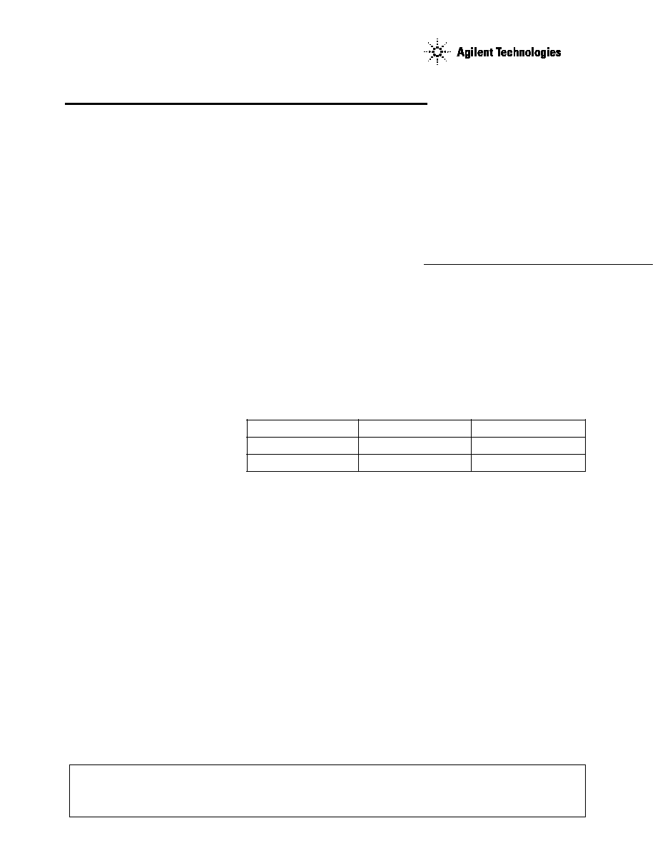
Solder Reflow Thermal Profile
Recommended Pb-Free IR Profile
0
TIME (SECONDS)
TEMPERATURE (
∞
C)
200
100
50
150
100
200
250
300
0
30
SEC.
50 SEC.
30
SEC.
160∞C
140∞C
150∞C
PEAK
TEMP.
245∞C
PEAK
TEMP.
240∞C
PEAK
TEMP.
230∞C
SOLDERING
TIME
200∞C
PREHEATING TIME
150∞C, 90 + 30 SEC.
2.5∞C ± 0.5∞C/SEC.
3∞C + 1∞C/≠0.5∞C
TIGHT
TYPICAL
LOOSE
ROOM
TEMPERATURE
PREHEATING RATE 3∞C + 1∞C/≠0.5∞C/SEC.
REFLOW HEATING RATE 2.5∞C ± 0.5∞C/SEC.
Insulation Related Specifications
Parameter
Symbol
Value
Units
Conditions
Min. External Air Gap
L(IO1)
5
mm
Measured from input terminals
(Clearance)
to output terminals
Min. External Tracking Path
L(IO2)
5
mm
Measured from input terminals
(Creepage)
to output terminals
Min. Internal Plastic Gap
0.08
mm
Through insulation distance
(Clearance)
conductor to conductor
Tracking Resistance
CTI
175
V
DIN IEC 112/VDE 0303 Part 1
Isolation Group (per DIN VDE 0109)
IIIa
Material Group DIN VDE 0109
217 ∞C
RAMP-DOWN
6 ∞C/SEC. MAX.
RAMP-UP
3 ∞C/SEC. MAX.
150 - 200 ∞C
260 +0/-5 ∞C
t 25 ∞C to PEAK
60 to 150 SEC.
20-40 SEC.
TIME WITHIN 5 ∞C of ACTUAL
PEAK TEMPERATURE
t
p
t
s
PREHEAT
60 to 180 SEC.
t
L
T
L
T
smax
T
smin
25
T
p
TIME
TEMPERA
TURE
NOTES:
THE TIME FROM 25 ∞C to PEAK
TEMPERATURE = 8 MINUTES MAX.
T
smax
= 200 ∞C, T
smin
= 150 ∞C

4
Electrical Specifications
Over recommended temperature (T
A
= 0
∞
C to 70
∞
C) unless otherwise specified. (See note 6.)
Parameter
Symbol Device Min. Typ.*
Max.
Units
Test Conditions
Fig.
Note
HCPL-
Current
CTR
M701
400
2000
3500
%
I
F
= 0.5 mA, V
O
= 0.4 V,
2, 3
1
Transfer
V
CC
= 4.5 V
Ratio
500
1600
2600
I
F
= 1.6 mA, V = 0.4 V,
V
CC
= 4.5 V
M700
300
1600
2600
I
F
= 1.6 mA, V
O
= 0.4 V,
V
CC
= 4.5 V
Logic Low
V
OL
M701
0.1
0.4
V
I
F
= 1.6 mA, I
O
= 8 mA,
1
Output
V
CC
= 4.5 V
Voltage
0.1
0.4
I
F
= 5 mA, I
O
= 15 mA,
V
CC
= 4.5 V
0.2
0.4
I
F
= 12 mA, I
O
= 24 mA,
V
CC
= 4.5 V
M700
0.1
0.4
I
F
= 1.6 mA, I
O
= 24 mA,
V
CC
= 4.5 V
Logic High
I
OH
M701
0.05
100
µ
A
I
F
= 0 mA,
Output
V
O
= V
CC
= 18 V
M700
0.1
250
I
F
= 0 mA,
V
O
= V
CC
= 7 V
Logic Low
I
CCL
0.4
1.5
mA
I
F
= 1.6 mA, V
O
= Open,
Supply
V
CC
= 18 V
Current
Logic High
I
CCH
0.01
10
µ
A
I
F
= 0 mA, V
O
= Open,
Supply
V
CC
= 18 V
Current
Input
V
F
1.4
1.7
V
T
A
= 25
∞
C
4
Forward
Voltage
1.75
I
F
= 1.6 mA
Input
BV
R
5
I
R
= 10
µ
A
Reverse
Breakdown
Voltage
Tempera-
V
F
/
T
A
-1.8
mV/
∞
C I
F
= 1.6 mA
ture Co-
efficient of
Forward
Voltage
Input
C
IN
60
pF
f = 1 MHz, V
F
= 0
Capacitance
Input-
V
ISO
3750
V
RMS
RH
50%, t = 1 min,
2, 3
Output
T
A
= 25
∞
C
Insulation
Resistance
R
I-O
10
12
V
I-O
= 500 V
DC
2
(Input-
Output)
Capacitance
C
I-O
0.6
pF
f = 1 MHz
2
(Input-
Output)
*All typicals at T
A
= 25
∞
C, V
CC
= 5 V.

5
Switching Specifications
Over recommended temperature (T
A
= 0
∞
C to 70
∞
C), V
CC
= 5 V, unless otherwise specified.
Sym- Device
Parameter
bol
HCPL- Min.
Typ.* Max. Unit
Test Conditions
Fig.
Note
Propagation
t
PHL
M701
25
75
µ
s
T
A
= 25
∞
C
I
F
= 0.5 mA,
5, 6,
100
7
0.5
2
T
A
= 25
∞
C
I
F
= 12 mA,
3
M700
5
20
T
A
= 25
∞
C
I
F
= 1.6 mA,
25
Propagation
t
PLH
M701
10
60
T
A
= 25
∞
C
I
F
= 0.5 mA,
5, 6,
90
7
1
10
T
A
= 25
∞
C
I
F
= 12 mA,
15
M700
10
35
T
A
= 25
∞
C
I
F
= 1.6 mA,
50
Common
|CM
H
|
1,000
10,000
V/
µ
s I
F
= 0 mA
8
4, 5
Mode
R
L
= 2.2 k
Transient
|V
CM
| = 10 V
p-p
Immunity at
Logic High
Output
Common
|CM
L
|
1,000
10,000
V/
µ
s I
F
= 1.6 mA
8
4, 5
Mode
R
L
= 2.2 k
Transient
|V
CM
| = 10 V
p-p
Immunity at
Logic Low
Output
*All typicals at T
A
= 25
∞
C.
R
L
= 4.7 k
R
L
= 270
R
L
= 2.2 k
R
L
= 4.7 k
R
L
= 270
R
L
= 2.2 k
Notes:
1. dc CURRENT TRANSFER RATIO in percent is defined as the ratio of output collector current, I
O
, to the forward LED input
current, I
F
, times 100.
2. Device considered a two terminal device: pins 1 and 3 shorted together, and pins 4, 5 and 6 shorted together.
3. In accordance with UL 1577, each optocoupler is proof tested by applying an insulation test voltage
4500 V
RMS
for 1 second
(leakage detection current limit, I
I-O
5
µ
A).
4. Common transient immunity in a Logic High level is the maximum tolerable (positive) dV
CM
/dt on the rising edge of the
common mode pulse, V
CM
, to assure that the output will remain in a Logic High state (i.e., V
O
> 2.0 V). Common mode transient
immunity in a Logic Low level is the maximum tolerable (negative) dV
CM
/dt on the falling edge of the common mode pulse
signal, V
CM
, to assure that the output will remain in a Logic Low state (i.e., V
O
< 0.8 V).
5. In applications where dV/dt may exceed 50,000 V/
µ
s (such as static discharge) a series resistor, R
CC
, should be included to
protect the detector IC from destructively high surge currents. The recommended value is R
CC
= 220
.
6. Use of a 0.1
µ
F bypass capacitor connected between pins 4 and 6 is recommended.
Delay Time
to Logic
Low at
Output
Delay Time
to Logic
High at
Output