CAUTION: It is advised that normal static precautions be taken in handling and assembly of this component
to prevent damage and/or degradation which may be induced by ESD.
0.4 Amp Output Current IGBT
Gate Drive Optocoupler
Technical Data
HCPL-T251
Features
∑ Supply Current
(I
CC
): 11 mA (Max.)
∑ Supply Voltage
(V
CC
): 10-30 V
∑ Output Current
(I
O
):
±
0.4 A (Min.)
∑ Switching Time
(t
PLH
/t
PHL
): 1
µ
s (Max.)
∑ Isolation Voltage
(V
ISO
): 3750 Vrms (Min.)
∑ UL 577 Recognized:
File No. E55361
∑ CSA Approved
∑ 10 kV/
µ
s Minimum Common
Mode Rejection (CMR) at
Vcm = 600 V
∑ Creepage Distance: 7.4 mm.
Clearance: 7.1 mm.
Applications
∑ IGBT/MOSFET Gate Drive
∑ AC/Brushless DC Motor
Drives
∑ Industrial Inverters
∑ Switch Mode Power
Supplies
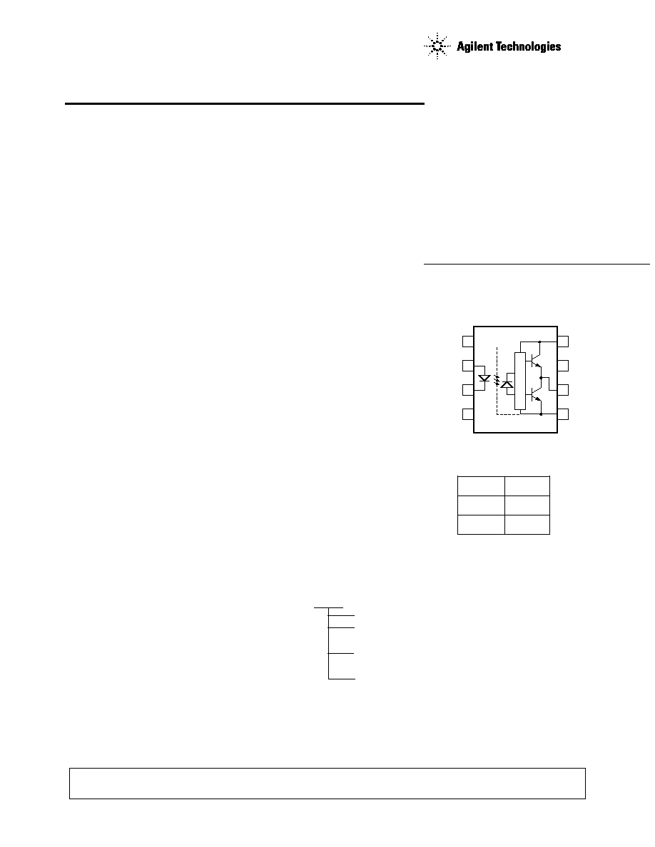
Description
The HCPL-T251 contains GaAsP
LED. The LED is optically
coupled to an integrated circuit
with a power output stage. This
optocoupler is ideally suited for
driving power IGBTs and
MOSFETs used in motor control
inverter applications. The high
operating voltage range of the
output stage provides the drive
voltages required by gate
controlled devices. The voltage
and current supplied by this
optocoupler makes it ideally
suited for directly driving small
or medium power IGBTs.
Ordering Information
Specify Part Number followed by
Option Number.
Example:
A 0.1
µ
F bypass capacitor must be connected between pins 5 and 8.
Functional Diagram
Truth Table
LED
V
out
OFF
LOW
ON
HIGH
HCPL-T251 #XXXX
No Option = Standard DIP Package, 50 per tube.
300 = Gull Wing Surface Mount Option,
50 per tube.
500 = Tape and Reel Packaging Option,
1000 per reel.
XXXE = Lead Free Option.
Remarks: The notation "#" is used for existing products, while (new)
products launched since 15th July 2001 and lead free option will use "-"
1
3
SHIELD
2
4
8
6
7
5
N/C
CATHODE
ANODE
N/C
VCC
VO
VO
VEE
2
Package Outline Drawings
Standard DIP Package
Gull Wing Surface Mount Option 300
1.080 ± 0.320
(0.043 ± 0.013)
2.54 ± 0.25
(0.100 ± 0.010)
0.51 (0.020) MIN.
0.65 (0.025) MAX.
4.70 (0.185) MAX.
2.92 (0.115) MIN.
5∞ TYP.
0.254
+ 0.076
- 0.051
(0.010
+ 0.003)
- 0.002)
7.62 ± 0.25
(0.300 ± 0.010)
6.35 ± 0.25
(0.250 ± 0.010)
9.65 ± 0.25
(0.380 ± 0.010)
1.78 (0.070) MAX.
1.19 (0.047) MAX.
A T251
YYWW
DATE CODE
DIMENSIONS IN MILLIMETERS AND (INCHES).
5
6
7
8
4
3
2
1
NOTE: FLOATING LEAD PROTRUSION IS 0.25 mm (10 mils) MAX.
3.56 ± 0.13
(0.140 ± 0.005)
PIN ONE
0.635 ± 0.25
(0.025 ± 0.010)
12∞ NOM.
9.65 ± 0.25
(0.380 ± 0.010)
0.635 ± 0.130
(0.025 ± 0.005)
7.62 ± 0.25
(0.300 ± 0.010)
5
6
7
8
4
3
2
1
9.65 ± 0.25
(0.380 ± 0.010)
6.350 ± 0.25
(0.250 ± 0.010)
1.016 (0.040)
1.27 (0.050)
10.9 (0.430)
2.0 (0.080)
LAND PATTERN RECOMMENDATION
1.080 ± 0.320
(0.043 ± 0.013)
3.56 ± 0.13
(0.140 ± 0.005)
1.780
(0.070)
MAX.
1.19
(0.047)
MAX.
2.54
(0.100)
BSC
DIMENSIONS IN MILLIMETERS (INCHES).
LEAD COPLANARITY = 0.10 mm (0.004 INCHES).
NOTE: FLOATING LEAD PROTRUSION IS 0.25 mm (10 mils) MAX.
0.254
+ 0.076
- 0.051
(0.010
+ 0.003)
- 0.002)
3
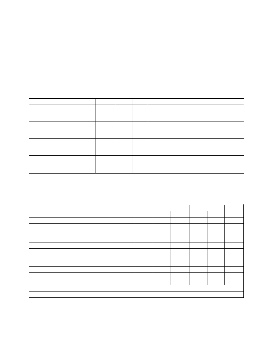
Regulatory Information
The HCPL-T251 is under
approval by the following
organizations:
UL
Approval under UL 1577,
Component Recognition
Program, File E55361.
Insulation and Safety Related
Parameter
Symbol
Value
Units
Conditions
Minimum External Air Gap
L(101)
7.1
mm
Measured from input terminals to
(Clearance)
output terminals, shortest distance through
air.
Minimum External Tracking
L(102)
7.4
mm
Measured from input terminals to
(Creepage)
output terminals, shortest distance path
along body.
Minimum Internal Plastic Gap
0.08
mm
Insulation thickness between emitter
(Internal Clearance)
and detector; also known as distance
through insulation
Tracking Resistance
CTI
175
Volts
DIN IEC 112/VDE 0303 Part 1
(Comparative Tracking Index)
Isolation Group
IIIa
Material Group (DIN VDE 0110, 1/89, Table 1)
Absolute Maximum Ratings
(Compared with HCPL-3140)
HCPL-3140
HCPL-T251
Parameter
Symbol
Units
Min.
Max.
Min.
Max.
Note
Operating Temperature
T
A
∞
C
- 40
100
-20
85
"High" Peak Output Current
I
OH(PEAK)
A
0.6
0.4
1
"High" Peak Output Current
I
OL(PEAK)
A
0.6
0.4
Storage Temperature
T
S
∞
C
-55
125
-55
125
Average Input Current
I
F(AVG)
mA
25
20
2
Peak Transient Input Current
I
F(TRAN)
A
1.0
1.0
(<1
µ
s Pulse Width, 300 pps)
Reverse Input Voltage
V
R
V
5
5
Supply Voltage
(V
CC
- V
EE
)
V
-0.5
35
-0.5
35
Output Voltage
V
O
V
0
V
CC
0
V
CC
Output Power Dissipation
P
O
mW
250
250
3
Lead Solder Temperature
260
∞
C for 10 sec., 1.6 mm below seating plane
Solder Reflow Temperature Profile
See Package Outline Drawings section
Notes:
1. Maximum pulse width = 10
µ
s, maximum duty cycle = 0.2%.
2. Derate linearly above 70
∞
C free-air temperature at a rate of 0.3 mA/
∞
C.
3. Derate lineraly above 70
∞
C free-air temperature at a rate of 4.8 mW/
∞
C.
CSA
Approval under CSA Component
Acceptance Notice #5, File CA 88324.
4
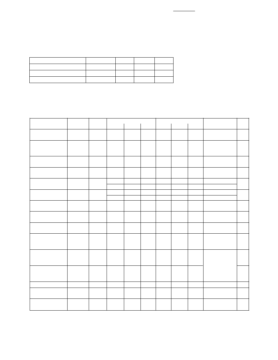
DC Electrical Specifications
(Compared with HCPL-3140)
Over recommended operating conditions (I
F(ON)
= 8 to 12 mA, V
F(OFF)
= 0 to 0.8 V, V
CC
= 15 to 30 V,
V
EE
= Ground) unless otherwise specified.
HCPL-3140
HCPL-T251
Test
Parameter
Symbol
Units
Min.
Typ.*
Max.
Min.
Typ.*
Max.
Conditions
Note
Input Forward
V
F
V
1.2
1.5
1.8
1.6
1.8
I
F
= 10 mA
Voltage
Temperature
V
F
/
T
A
mV/
∞
C
-1.6
-2.0
I
F
= 10 mA
Coefficient of
Forward Voltage
Input Reverse
I
R
µ
A
10
10
V
R
= 5 V
Current
Input Capacitance
C
IN
pF
60
45
250
V
F
= 0 V,
F = 1 MHz
High Level
I
OH
A
0.2
0.25
V
O
= V
CC
- 4 V
Output Current
0.4
0.5
N.A.
V
O
= V
CC
- 15 V
Low Level
I
OL
A
0.2
0.4
0.1
0.2
V
O
= V
CC
- 4 V
Output Current
0.4
0.5
N.A.
V
O
= V
CC
- 15 V
High Level
V
OH
V
V
CC
- 4 V
CC
- 1.8
V
CC
- 4 V
CC
- 1.8
I
O
= -100 mA
Output Voltage
Low Level
V
OL
V
0.4
1
0.5
I
O
= 100 mA
Output Voltage
High Level
I
CCH
mA
0.7
3
7.5
11
Output Open
Supply Current
ntSupply Current
I
F
= 7 to 16 mA
Low Level
I
CCL
mA
1 - 2
3
8
11
Output Open
Supply Current
V
F
= -3.0 to
+0.8 V
Threshold Input
I
FLH
mA
6
7
I
O
= 0 mA,
Current Low to
V
O
> 5 V
High
Threshold Input
V
FHL
V
0.8
0.8
Voltage High
to Low
Supply Voltage
V
CC
V
10
30
10
30
Capacitance
C
I-0
pF
60
60
(Input-Output)
Resistance
R
I-0
10
12
10
12
(Input-Output)
*All typical values at T
A
= 25
∞
C and V
CC
- V
EE
= 3
∞
V, unless otherwise noted.
Recommended Operating Conditions
Parameter
Symbol
Min.
Max.
Units
Power Supply Voltage
V
CC
- V
EE
15
30
V
Input Current (ON)
I
F(ON)
8
12
mA
Input Voltage (OFF)
V
F(OFF)
0
0.8
V

5
Switching Specifications (AC)
(Compared with HCPL-3140)
Over recommended operating conditions (T
A
= -40 to 100
∞
C, I
F(ON)
= 8 to 12 mA, V
F(OFF)
= -3.0 to 0.8 V,
V
CC
= 15 to 30 V, V
EE
= Ground) unless otherwise specified.
HCPL-3140
HCPL-T251
(-40
∞
C ~ 100
∞
C)
(-20
∞
C ~ 70
∞
C)
Test
Parameter
Symbol Units
Min.
Typ.*
Max.
Min.
Typ.*
Max.
Conditions
Note
Propagation Delay
t
PHL
µ
s
0.1
0.2
0.7
0.25
1
Time to High
Output Level
Propagation Delay
T
PLH
µ
s
0.1
0.3
0.7
0.25
1
Time to Low
Output Level
Output Rise Time
t
R
ns
50
N.A.
Output Fall Time
t
F
ns
50
N.A.
Propagation
(t
PHL
-
µ
s
-0.5
0.5
N.A.
N.A.
4
Delay Difference
t
PLH
)
Between Any
PDD
Two Parts
Output High
|CM
H
|
kV/
µ
s
10
10
T
A
= 25
∞
C
5
Level Common
V
CC
= 30 V
Mode Transient
HCPL
I
F
= 10 mA
Immunity
-3140
V
CM
= 1000 V
HCPL
I
F
= 8 mA
-T251
V
CM
= 600 V
Output Low
|CM
L
|
kV/
µ
s
10
10
T
A
= 25
∞
C
5
Level Common
V
F
= 0 V
Mode Transient
HCPL
Immunity
-3140
V
CM
= 1000 V
HCPL
-T251
V
CM
= 600 V
*All typical values at T
A
= 25
∞
C and V
CC
- V
EE
= 30 V, unless otherwise noted.
Notes:
4. The difference between t
PHL
and t
PLH
between any two HCPL-3140 parts under the same test condition.
5. Common mode transient immunity in the high state is the maximum tolerable dV
CM
/dt of the common mode pulse, V
CM
, to assure
that the output will remain in the high state (i.e., V
O
> 15.0 V).
6. Common mode transient immunity in a low state is the maximum tolerable dV
CM
/dt of the common mode pulse, V
CM
, to assure that
the output will remain in a low state (i.e., V
O
< 1.0 V).
Rg = 47
Cg = 3 nF,
f = 10 kHz,
Duty Cycle = 50%