 | –≠–ª–µ–∫—Ç—Ä–æ–Ω–Ω—ã–π –∫–æ–º–ø–æ–Ω–µ–Ω—Ç: HDCS-1020 | –°–∫–∞—á–∞—Ç—å:  PDF PDF  ZIP ZIP |
Agilent HDCS-1020, HDCS-2020
CMOS Image Sensors
Data Sheet
Description
The HDCS-1020 and HDCS-2020
CMOS Image Sensors capture high
quality, low noise images while
consuming very low power. These
parts integrate a highly sensitive
active pixel photodiode array with
timing control and onboard A/D
conversion. Available in either
VGA (640 x 480) or CIF (352 x 288)
resolution image arrays, the
devices are ideally suited for a
wide variety of applications.
The HDCS-2020 and HDCS-1020,
when coupled with Agilent's
HDCP family of image processors,
provide a complete imaging
system to enable rapid end-
product development. Designed
for low-cost consumer electronic
applications, the HDCS-2020 and
HDCS-1020 sensors deliver
unparalleled performance for
mainstream imaging applications.
HDCS-2020 (VGA) and
HDCS-1020 (CIF) are CMOS active
pixel image sensors with inte-
grated A/D conversion and full
timing control. They provide
random access of sensor pixels,
which allows windowing and
panning capabilities. The sensor is
designed for video conferencing
applications and still image
capabilities. The HDCS family
Key Specifications and Features
∑ Available in two image array sizes:
VGA (640 x 480) and CIF (352 x 288)
∑ RGB Bayer color filter array
∑ Independent X and Y sub-sampling
modes (2:1 each) providing up to a
4X frame rate increase
∑ HDCS-1020 Full frame video rate at
8 bit resolution: 30 fps CIF at
32 MHz and 25.8 fps at 25 MHz
∑ HDCS-2020 Full frame video rates
at 10 bit resolution: 15 fps VGA at
25 MHz
∑ Still image capability
∑ Mechanical shutter and external
flash mode
∑ Low power modes
∑ Shadow gain and exposure
registers
∑ Integrated analog to digital
converters: HDCS-2020 (10 bit),
HDCS-1020 (8 bit)
∑ Automatic subtraction of column
fixed pattern noise
∑ Integrated voltage references
∑ Digital image data output via 8 bit
(HDCS-1020) and 10 bit (HDCS-2020)
synchronous parallel interface or
serial interface
Applications
∑ Digital still cameras
∑ PC cameras
∑ Handheld computers
∑ Cellular phones
∑ Notebook computers
∑ Toys
achieves excellent image quality
with very low dark current, high
sensitivity, and superior anti-
blooming characteristics. The
devices operate from a single DC
bias voltage, are easy to configure
and control, and feature low
power consumption.
Programmable Features
∑ Programmable window size
ranging from the full array down to
a 4 x 4 pixel window
∑ Programmable panning capability
which allows a specified window
(minimum 4 x 4 pixels) to be located
anywhere on the sensor array
∑ Integrated programmable gain
amplifiers with independent gain
control for each color (R, G, B)
∑ Internal register set programmable
via either the UART or synchronous
serial interface
∑ Integrated timing controller with
rolling electronic shutter, row/
column addressing, and operating
mode selection with programmable
exposure control, frame rate, and
data rate
∑ Programmable horizontal, vertical,
and shutter synchronization signals
∑ Programmable horizontal and
vertical blanking intervals

2
Introduction to Sensor Use
The sensor acts as a normal CMOS
digital device from the outside.
Internal circuits are a combination
of sensitive analog and timing
circuits. Therefore, the designer
must pay attention to the PC
board layout and power supply
design. Writing to registers via an
I
2
C compatible two-wire interface
provides control of the sensor.
Sensor data is normally output via
an 8 or 10 bit parallel interface
(serial data output is also avail-
able). Once the registers are
programmed the sensor is self-
clocking and all timing is inter-
nally generated. On chip program-
mable amplifiers provide a way to
separately adjust the red green
and blue pixels for a good white
balance. Analog to digital conver-
sion is also on chip and 8 or 10 bit
digital data is output. A data ready
pulse follows each valid pixel
output. An end of row signal
follows each row and an end of
frame signal follows each frame.
PCB Layout
Analog Vdd and analog ground
need to be routed separately from
digital Vdd and digital ground.
Noisy circuits or ICs should not be
placed on the opposite side of the
PC board. Heat producing circuits
such as microprocessors or LCD
displays should not be placed next
to or opposite from the sensor to
reduce noise in the image.
Power Supply
The sensor operates at 3.3 VDC.
There are two power supplies for
the sensor, analog Vdd and digital
Vdd. The two supplies and
grounds must be kept separate.
Two separate regulators provide
the best isolation. Any noise on
the analog supply will result in
noise in the image. Analog and
digital ground should be tied
together at a single point of lowest
impedance and noise.
Master Clock
The part requires a 50% duty cycle
master clock. Maximum clock
rates are 25 MHz for HDCS-2020
and 32 MHz for HDCS-1020.
Reset
A hard reset is required before the
sensor will function properly.
Once the master clock is running,
assert nRST_nSTBY for 40 clock
cycles.
Register Communication
Communication (read/write) to
the sensor registers is via a two
wire serial interface-- either a
synchronous I
2
C compatible or
half duplex UART (9600 baud
default). nTristate (pin 15
HDCS-1020 only) must be pulled
high for normal operation. The
HDCS-2020 does not have
nTristate.
Parallel Data Output
8 or 10 bit parallel data is output
from the sensor. A data ready line
(DRDY) is asserted when the data
is valid. The sensor acts as a
master in the way it outputs data.
There is no flow control or data
received handshake. Once the RUN
bit (CONTROL register) is set, the
image processor must be ready to
accept data at the sensor rate and
when the data is presented.
Serial Data Output
In this mode, output data lines D0
and D1 (the lower two bits of the
parallel data port) act as a two
wire serial interface.
Handshaking
At the end of one row of data,
the nROW line is asserted. At the
end of one frame of data, the
nFRAME_nSYNC line is asserted.
Registers
The following is a table of sample
register settings. These values are
a good starting point.

3
Table 1. Register Set Declaration.
Register Name
Mnemonic
Address (hex)
Sample Value (hex)
Identifications Register
IDENT
0x00
Status Register
STATUS
0x01
0x7F
Interrupt Mask Register
IMASK
0x02
0x00
Pad Control Register
PCTRL
0x03
0x03
Pad Drive Control Register
PDRV
0x04
0x00
Interface Control Register
ICTRL
0x05
0x20
Interface Timing Register
ITMG
0x06
0x00
Baud Fraction Register
BFRAC
0x07
0x00
Baud Rate Register
BRATE
0x08
0x00
ADC Control Register
ADCCTRL
0x09
0x08
First Window Row Register
FWROW
0x0A
0x00
First Window Column Register
FWCOL
0x0B
0x07
Last Window Row Register
LWROW
0x0C
0x79
Last Window Column Register
LWCOL
0x0D
0xA8
Timing Control Register
TCTRL
0x0E
0x04
PGA Gain Register: Green
ERECPGA
0x0F
0x00
PGA Gain Register: Red
EROCPGA
0x10
0x00
PGA Gain Register: Blue
ORECPGA
0x11
0x00
PGA Gain Register: Green
OROCPGA
0x12
0x00
Row Exposure Low Register
ROWEXPL
0x13
0x00
Row Exposure High Register
ROWEXPH
0x14
0x02
Sub-Row Exposure Register
SROWEXP
0x15
0x00
Error Control Register
ERROR
0x16
0x00
Interface Timing 2 Register
ITMG2
0x17
0x4B
Interface Control 2 Register
ICTRL2
0x18
0x00
Horizontal Blank Register
HBLANK
0x19
0x00
Vertical Blank Register
VBLANK
0x1A
0x00
Configuration Register
CONFIG
0x1B
0x0C
Control Register
CONTROL
0x1C
0x04
Reserved
0x1D
--
Reserved
0x1E
--
Reserved
0x1F
--
Reserved
0x20
--

4
Setting Exposure and Gain
The exposure of an image is a
function of the exposure and gain
registers. Exposure sets the length
of time each pixel integrates the
light (shutter speed). Gain settings
allow pixel values to be amplified.
Gain values from 1x to 40x are
allowed, but higher gain settings
amplify noise (much like higher
ISO film speeds are grainier). It is
best to use the lower gain settings
for better images. Gains from 1x to
10x are generally recommended.
Note there are two green gain
registers listed in Table 2, one for
the odd number row green pixels
and one for the even number row
green pixels. The green color
filters can be slightly different
between rows and this allows fine-
tuning. Using the same gain
setting for both green registers is
usually enough. Since the blue
channel is not as sensitive, using
blue gains approximately double
that of red and green will allow
the A/D full range on all three
channels.
Using a MacBeth Color Checker is
a good way to judge exposure and
color balance. A good raw image
will have a good grey scale (the
bottom patches on the chart).
Gain settings should be adjusted
so the red, green, and blue values
are equal on any one grey patch.
After setting gain, the exposure
registers should be adjusted for a
good exposure. There are three
exposure registers; see Table 3.
Table 2.
Register Name
Mnemonic
Address (hex)
PGA Gain Register: Green
ERECPGA
0x0F
PGA Gain Register: Red
EROCPGA
0x10
PGA Gain Register: Blue
ORECPGA
0x11
PGA Gain Register: Green
OROCPGA
0x12
Table 3.
Register Name
Mnemonic
Address (hex)
Row Exposure Low Register
ROWEXPL
0x13
Row Exposure High Register
ROWEXPH
0x14
Sub-Row Exposure Register
SROWEXP
0x15
The row exposure high register
(upper 8 bits) and row exposure
low register (lower 8 bits) act as a
single 16 bit register. This 16 bit
register sets the integration time
(shutter speed) of the sensor. The
sub-row exposure register is used
for very small changes to expo-
sure and allow fine-tuning for
exact shutter speeds.
Proper exposure will result in
black values near 0x00 and white
values near 0xFF (assuming
8 bits). All six grey patches on the
MacBeth chart should have
different average intensity values
in the image. If the two brightest
patches both appear white then
the exposure is too long. If the
two darkest patches both appear
black then the exposure is too
short. Remember that the raw
image does not have gamma
correction applied yet. The final
grey scale image needs to be
evaluated after gamma correction.
Image Processing
The raw data from the sensor
requires image processing before
a digital image is ready for view-
ing. Some standard steps of image
processing are as follows:
1. Defective pixel correction
2. Lens flare subtraction
3. Auto-exposure
4. Auto-white balance
5. Color filter array interpolation
(demosaic)
6. Color correction (3x3 matrix)
7. Gamma correction
8. Color space correction
(3x 3 matrix)
9. Data compression
Image processing is not part of the
sensor and must be supplied
separately. Image processors
that are compatible with these
sensors are available from Agilent
Technologies (HDCP-2000,
HDCP-2010).
5
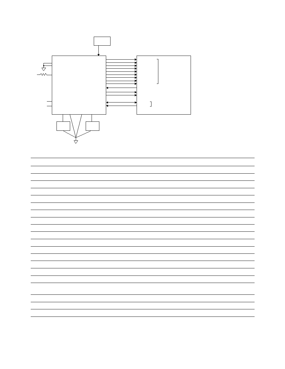
Typical Application
Typical Electrical Specifications
Part Number
HDCS-2020 (VGA)
HDCS-1020 (CIF)
Pixel size
7.4 x 7.4
µ
m
7.4 x 7.4
µ
m
Maximum Clock Rate
25 MHz (VGA)
32 MHz (CIF)
Effective Sensor Dynamic Range
65 dB (VGA)
61 dB (CIF)
Effective Noise Floor
43 e-
43 e-
Dark Signal
[1,4]
240 e-/sec (@ 22
∞
C)
240 e-/sec (@ 22
∞
C)
Sensitivity
[2,3]
1.1 V/(Lux-S)
1.1 V/(Lux-S)
Peak Quantum Efficiency
[1,2,3]
33%
33%
Saturation Voltage
1.22 V
1.22 V
Full Well Capacity
68,000 e-
68,000 e-
Conversion Gain
[2]
17
µ
V/e-
17
µ
V/e-
Programmable Gain Range
1 ≠ 40 (8 bit resolution)
1≠ 40 (8 bit resolution)
Fill Factor
42%
42%
Exposure Control
0.5
µ
sec minimum, 0.5
µ
sec increments
0.5
µ
sec minimum, 0.5
µ
sec increments
Supply Voltage
3.3 V, -5%/+10%
3.3 V, -5%/+10%
Absolute Max. Power Supply Voltage
3.6 V
3.6 V
Absolute Max. DC Input Voltage (any pin)
3.6 V
3.6 V
Power Consumption (typical)
150 mW operating, 150
µ
W standby
150 mW operating, 150
µ
W standby
Power Consumption (max)
200 mW operating, 3.3 mW standby
200 mW operating, 3.3 mW standby
Optical Format
1/3"
1/4"
Operating Temperature
-5
∞
to +65
∞
C
-5
∞
to +65
∞
C
Storage Temperature
-40
∞
to +125
∞
C
-40
∞
to +125
∞
C
Notes:
1. Specified over complete pixel area
2. Measured at unity gain
3. Measured at 555 nm
4. Excludes dark current shot noise
IMODE0
IMODE1
nTRISTATE
nIRQ
3.3V
Regulator
NC
Clock
Serial Interface
Host System
HDCS-1020
TxD/RxD
Analog
Vdd
Analog
GND
Digital
GND
Digital
Vdd
nFRAME_nSYNC
nROW
nRST_nSTBY
End of Frame
End of Row
Reset
D0
D1
D2
D3
D4
D5
D6
D7
DATA READY
D0
D1
D2
D3
D4
D5
D6
D7
DRDY
24
23
22
3, 20,
28
4, 11, 17
30
29
26
21
2, 19,
27
5, 12,
18
Star Ground
16
25
10K
Vdd
NC
NC
3.3V
Regulator
31
6
1
32
9
8
13
10
14
7
Clk
30 MHz
Clock
25
Parallel Interface