
Agilent HDJD-J822-SCR00
Color Management System
Feedback Controller
Data Sheet
Features
∑ ≠40 to 85∞C operation
∑ I
2
C serial interface
∑ Robust CMOS-Schmitt input
∑ CMOS/TTL compatible output
∑ Multiple color input formats ≠
CIE XYZ, Yxy, Yu'v' and RGB
∑ 3-channel analog interface to
color sensor ≠ X, Y and Z channels
∑ 3-channel 12-bit PWM output ≠
Red, Green, and Blue LED channels
∑ Internal computation of calibration
data
∑ Internal clock generator
∑ Internal reference voltage
generator
∑ Error flag output
∑ External push-button interface
∑ Only passive components required
externally
Applications
∑ Backlighting
∑ General illumination
∑ Mood/accent lighting
∑ Color context sensitive appliances
Description
The HDJD-J822 is a CMOS mixed-
signal IC designed to be the
optical feedback controller of an
LED-based lighting system. A
typical system consists of an
array of red, green and blue
LEDs, LED drivers, a tri-color
photosensor that samples the
light output, and the HDJD-J822.
The IC interfaces directly to the
photosensor, processes the color
information and adjusts the light
output from the LEDs until the
desired color is achieved. To
achieve this, the IC integrates a
high-accuracy 10-bit analog-to-
digital converter front-end, a
color data processing logic core,
and a high-resolution 12-bit PWM
output generator.
By employing a feedback system
and the HDJD-J822, the light
output produced by the LED
array maintains its color over
time and temperature. In
addition, the desired color can be
specified using a standard CIE
color space.
In addition, by incorporating a
standard I
2
C serial interface,
specifying the color of the LED
array's light output is as simple as
picking the color coordinates
from the CIE color space and
writing several bytes of data to
the device.
The output PWM signals are
connected directly to the LED
drivers as enable signals. The
PWM signals control the on-time
duration of the red, green and
blue LEDs. That duration is
continually adjusted in real-time
to match the light output from the
LED array to the specified,
desired color.

4
Pin Descriptions
XRST (Pin 1)
Global, asynchronous, active-low
system reset. When asserted low,
XRST resets all registers.
Minimum reset pulse low is
10
µs and must be provided by
external circuitry.
SLEEP (Pin 2)
When asserted high, SLEEP puts
the device into sleep mode. In
sleep mode, all analog circuits are
powered down and the clock
signal is gated away from the core
logic.
CLK_SEL (Pin 3)
CLK_SEL is used to select
between internal and external
clock modes. Internal clock mode
is selected when CLK_SEL=0 and
external clock mode is selected
when CLK_SEL=1.
A1, A0 (Pin 4, Pin 5)
A1 (MSB) and A0 (LSB) define the
lower two bits of the I
2
C slave
address.
SDA (Pin 6)
The SDA pin is the I
2
C data I/O
pin. SDA is a bi-directional pin.
The I/O direction is defined by an
internal signal generated by the
I
2
C interface block.
SCL (Pin 7)
The SCL pin is the I
2
C clock pin.
TEST (Pin 8)
Connect to digital ground (DVSS).
COLOR, BRIGHT (Pin 9, Pin 10)
COLOR and BRIGHT are button
interface pins. Asserting COLOR
high with BRIGHT low makes the
output color go up a color
selection `slider.' To effect a
direction change, COLOR and
BRIGHT must be asserted
simultaneously for at least 0.1
second. Now, asserting COLOR
with BRIGHT low makes the
output color go down the color
selection slider.
Button brightness control follows
a similar procedure. Asserting
BRIGHT high with COLOR low
increases or decreases brightness
depending on the direction. To
effect a direction change, COLOR
and BRIGHT must be asserted
simultaneously for at least 0.1
second. (Refer to Application
Note 5070
for color selection
`slider.')
CLK_EXT (Pin 11)
CLK_EXT is the external clock
input pin. Users can choose to
use an external clock instead of
the internal clock generator by
setting CLK_SEL to high.
PWM_R, PWM_G, PWM_B (Pin 16,
Pin 15, Pin 14)
The PWM_R, PWM_G, and
PWM_B output pins drive the
external LED drivers that drive
the LED arrays. Typically PWM_R
drives only the red LEDs, PWM_G
drives only the green LEDs and
PWM_B drives only the blue
LEDs. They are the output enable
signals of the red, green and blue
LED drivers. So, they control the
on-time duration of the LEDs.
The assertion level of the PWM*
signals can be toggled by the user
to support both active-low and
active-high enable input pins at
the LED driver side. This is done
by configuring the PWML bit of
register CONFIG1.
ERR_FLAG (Pin 17)
The ERR_FLAG pin is asserted
high when an error condition is
detected. The user can determine
the type of error by reading the
ERROR register. The error
conditions are described in the
`High Level Description' section.
SENSE_X, SENSE_Y, SENSE_Z (Pin
23, Pin 22, Pin 21)
The SENSE_X, SENSE_Y and
SENSE_Z pins are analog input
pins which are tied to the
X-channel, Y-channel and
Z-channel of the photosensor
output respectively. An averaging
filter is placed in between the
sensor output and the SENSE_X,
SENSE_Y and SENSE_Z pins. The
filter is typically a 68 k
-1 µF
single-pole low-pass filter.
VREF_EXT (Pin 20)
The VREF_EXT pin is an analog
input pin, which provides an
external reference voltage for the
ADC. Typically, users will use the
internal reference generator to
operate the ADC. However, in
specific application conditions,
an external reference may be
required. The external reference
is enabled by setting the VREFS
bit of register CONFIG1 high.
ROSC (Pin 19)
A 68 k
precision 1% resistor is
connected from the ROSC to
AVSS pin for use by the internal
oscillator. In external clock
mode, ROSC can be left floating.
(Refer to Application Note 5070
for resistor selection.)
DVDD, DVSS, AVDD, AVSS (Pin 12,
Pin 13, Pin 24, Pin 18)
HDJD-J822 has separate power
ground nets for the analog and
digital section. A star connection
from a central power source is
recommended when designing
the wiring to these supply pins.
DVDD = Digital positive supply
DVSS = Digital ground
AVDD = Analog positive supply
AVSS = Analog ground
5
General Specifications
Feature
Value
Interface
I
2
C 100 kHz
Input Color Format
CIE XYZ, Yxy, Yu'v' and RGB (illuminant E)
Input Sensor Signal
0 to 2.5 V (typical configuration)
Minimum Dynamic Range
Sensor output > 500 (ADC output code, each channel)
during calibration
Output PWM Frequency
610 Hz nominal (typical configuration)
Output PWM Resolution
12 bits
Error Flag
Assertion on ERR_FLAG pin indicates an error condition
Device Address Control
Upper 5 bits 10101 binary, lower 2 bits defined by
A1:A0 pins in that order
Supply
5 V digital, 5 V analog (nominal)
I/O
Schmitt-CMOS input and CMOS/TTL compatible output
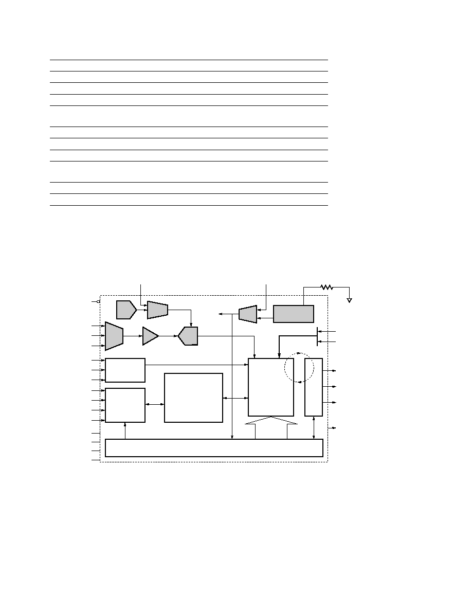
Block Diagram
XRST
AVDD
SLEEP
SENSE_X
CLK_SEL
SENSE_Y
A1
SENSE_Z
A0
VREF_EXT
MODE SELECT
VREF
SENSOR
PROGRAMMABLE
AMPLIFIER
REFERENCE
VOLTAGE
ADC
MUX
CLOCK
SDA
ROSC
SCL
AVSS
TEST
ERR_FLAG
COLOR
PWM_R
BRIGHT
PWM_G
CLK_EXT
PUSH_BUTTON
DUTY FACTOR
SYSTEM CONTROLLER
CONTROL
SIGNALS
PWM_B
PWM GENERATOR
DVDD
DVSS
INTERNAL
OSCILLATOR
COLOR
CONTROLLER
INTERNAL REGISTERS
CONTROL
CONFIG
DATA:
SETPOINT
CALIBRATION
I2C
INTERFACE
CONTROL

