 | –≠–ª–µ–∫—Ç—Ä–æ–Ω–Ω—ã–π –∫–æ–º–ø–æ–Ω–µ–Ω—Ç: HDMP-1514 | –°–∫–∞—á–∞—Ç—å:  PDF PDF  ZIP ZIP |
Document Outline
- Features
- Applications
- Description
- List of Figures
- 1. Point-to-Point Data Link.
- 2. HDMP-1512 (Tx) Block Diagram.
- 3. Laser Driver Block Diagram and External Circuitry.
- 4. LZDC Equivalent Output Circuit (Tx pin # 21)
- 5. HDMP-1514 (Receiver) Block Diagram.
- 6. Simple Circuit Used to Adjust the Voltage on Rx pin # 21, DR_REF.
- 7. Typical Frequency Response Plot of the Internal Input Equalizer
- 8. Typical Plot of Loss of Light Threshold Voltage vs. DR_ REF Voltage
- 9. O-TTL and I-TTL Simplified Circuit Schematic.
- 10. O-BLL and I-H50 Simplified Circuit Schematics. (Note: I-H50 Inputs Should Never Be Connected to Ground. . .
- 11. HDMP-1512 (Tx) Package Layout, Top View.
- 12. HDMP-1514 (Rx) Package Layout.
- 13. HDMP-1512 and HDMP-1514 Package Outline.
- 14. HDMP-1512 (Transmitter) Timing Diagram, with PPSEL = 0.
- 15. HDMP-1514 (Receiver) Timing Diagram, with PPSEL = 0.
- 16. HDMP-1512 (Transmitter) Timing Diagram In Ping-Pong Mode, PPSEL = 1.
- 17. HDMP-1514 (Receiver) Timing Diagram in Ping-Pong Mode, with PPSEL = 1.
- 18. Typical Transmitter Pin Terminations for Applications Requiring High Speed Serial Copper Drivers (± So).
- 19. Typical Transmitter Pin Terminations for Applications Using the On-Chip Laser Driver. For Details of the Laser Driver. . .
- 20. Typical Receiver Pin Terminations for Applications Using High Speed Serial Copper Links (± DIN).
- 21. Typical Receiver Pin Terminations for Applications Using High Speed Fiber Links (± DIN).
- Transmitter Operation
- HDMP-1512 Input Output Select Table
- Transmitter Laser Driver Operation
- Receiver Operation
- Rx Power Supply Supervisor
- Recommended Handling Precautions
- HDMP-1512 (Tx), HDMP-1514 (Rx) Absolute Maximum Ratings
- HDMP-1512 (Tx), HDMP-1514 (Rx) Specified Operating Rates
- HDMP-1512 (Tx), HDMP-1514 (Rx) Transmitter & Receiver Byte Rate Clock Requirements
- HDMP-1512 (Tx), HDMP-1514 (Rx) AC Electrical Specifications
- HDMP-1512 (Tx) Output Jitter Characteristics
- HDMP-1512 (Tx), HDMP-1514 (Rx) DC Electrical Specifications
- HDMP-1512 (Tx) Laser Driver Characteristics
- HDMP-1512 (Tx) Timing Characteristics
- HDMP-1514 (Rx) Timing Characteristics
- HDMP-1512 (Tx), HDMP-1514 (Rx) Thermal Characteristics
- I/O Type Definitions
- HDMP-1512 (Tx)Pin Assignments
- HDMP-1512 (Tx), Signal Definitions
- HDMP-1514 (Rx) Pin Assignments
- HDMP-1514 (Rx), Signal Definitions
- Package Description and Assembly Recommendations
- M-Quad 80 Package Specifications

656
Fibre Channel Transmitter and
Receiver Chipset
Technical Data
HDMP-1512 Transmitter
HDMP-1514 Receiver
Features
∑ ANSI X3.230-1994 Fibre
Channel Standard
Compatible (FC-0)
∑ Selectable 531.25 Mbaud or
1062.5 Mbaud Data Rates
∑ Selectable On Chip Laser
Driver and 50
Cable
Driver
∑ TTL Compatible I/Os
∑ Single +5.0 V Power Supply
Applications
∑ Mass Storage System I/O
Channel
∑ Work Station/Server I/O
Channel
∑ High Speed Peripheral
Interface
Description
The HDMP-1512 transmitter and
the HDMP-1514 receiver are
bipolar integrated circuits,
separately packaged, in 80 pin M-
Quad packages. They are used to
build a high speed Fibre Channel
link for point to point data com-
munications. Shown in Figure 1 is
a typical full duplex point-to-
point Fibre Channel link. The
sending system provides parallel,
8B/10B, encoded data and a
transmit byte clock to the HDMP-
1512 transmitter. Using the trans-
mit byte clock, the transmitter
converts the data to a serial
stream and sends it over a copper
cable or fiber-optic link. The
receiver converts the serial data
stream back to parallel encoded
data and presents it, along with
the recovered transmit byte
clock, to the receiving system.
The sending system has the
option to electrically wrap the
transmitted data back to the local
receiver. It is possible to transmit
over the cable driver, or laser
driver when data is being
wrapped back to the local
receiver.
The two-chip set (transmitter
chip and receiver chip) is
compatible with the FC-0 layer of
the American National Standards
Institute (ANSI), Fibre Channel
specification, X3.230-1994. This
specification defines four
standard rates of operation for
Fibre Channel links. The HDMP-
1512 and HDMP-1514 chip-set
will operate at the two highest
defined serial rates of 531.25
Mbaud and 1062.5 Mbaud. These
serial baud rates correspond to
8B/10B encoded byte rates of 50
Mbytes/sec and 100 Mbytes/sec
respectively. The proper setting
of a single pin on each chip
selects the desired rate of
operation.
Several features, exclusive to this
chip-set, make it ideal for use in
Fibre Channel links. In addition,
the laser driver on the transmitter
chip, the dual loss of light
detectors on the receiver chip,
and the power supervisor and
power reset features make this
chip-set ideal for use with laser
optics. The serial cable driver
(transmitter chip), and the cable
equalizer (on the receiver chip),
can be operated in conjunction
with, or as an alternative to, the
laser driver. The laser driver can
also be driven directly with an
external high speed serial input.
Altogether, the various features,
input/output options, and
flexibility of this chip-set make
several unique link configurations
possible. In particular, it is ideally
suited for use in applications
where conformance to the FCSI
specification # 301-Rev 1.0,
Gbaud Link Module Specification,
is desired.
5964-6637E (4/96)

657
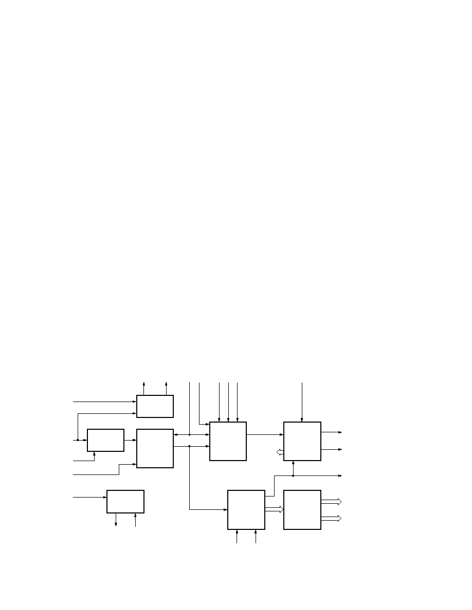
Figure 2. HDMP-1512 (Tx) Block Diagram.
TTL INTERFACE
AND
INPUT LATCH
DATA BYTE 1
Tx [10:19]
± SI
DATA BYTE 0
Tx [00:09]
FRAME
MULTIPLEXER
10
10
20
I/O
SELECT
CABLE
DRIVERS
± LOUT
± SO
PLL/CLOCK
GENERATOR
TBC
LASER
DRIVER
INTERNAL
CLOCKS
2
2
± LZOUT
2
LASER
CONTROLS
TS2
TS1
EWRAP
PPSEL
SPDSEL
-LZON
FAULT
-COMGEN
Transmitter Operation
The block diagram of the HDMP-
1512 transmitter is shown in
Figure 2. The basic functions of
the transmitter chip are the TTL
Interface and Input Latch, Frame
Multiplexing, Input/Output
selection, cable drivers, Laser
Driver, and monolithic Phase
Locked loop clock generator. The
actual operation of each function
changes slightly, according to the
desired configuration and option
settings. Figures 18 and 19 show
schematically how to terminate
each pin on the HDMP-1512
when used in systems incorporat-
ing either copper or fiber media.
There are two main modes of
operation for the transmitter
chip, both are based on the
selected baud rate. The baud rate
is controlled by the appropriate
setting of the SPDSEL pin, #67.
When this pin is set low, the
transmitter operates at a serial
rate of 531.25 Mbaud. When pin
#67 is set high the transmitter
operates at a serial rate of 1062.5
Mbaud. As such, the two main
modes of operation are the
531.25 Mbaud mode and the
1062.5 Mbaud mode.
The transmitter does not encode
the applied data. It assumes the
data is pre-encoded using the
8B/10B encoding scheme as
defined in ANSI X3.230-1994.
The TTL input interface receives
data at the standard TTL levels
specified in the dc Electrical
Specification table. The internal
phase locked loop (PLL) locks to
the transmit byte clock, TBC.
TBC is supplied to the transmitter
chip by the sending system. TBC
should be a 53.125 MHz clock
(
±
100 ppm) as defined in
X3.230-1994. Once the PLL has
locked to TBC, all the clocks used
by the transmitter are generated
by the internal clock generator.
CLOCK
Tx
Rx
ENCODED DATA
CLOCK
ENCODED DATA
REF CLOCK
Rx
Tx
CLOCK
ENCODED DATA
CLOCK
ENCODED DATA
REF CLOCK
SERIAL LINK
SERIAL LINK
Figure 1. Point-to-Point Data Link.

658
tions of 10 bit binary words, the
8B/10B code reserves 256 of
them to represent the valid
combinations of 8 bit data. Some
of the remaining combinations
are reserved for special functions.
The character reserved for
defining the transmitted word
boundary has been defined as the
K28.5 character, also known as a
comma character. The receiver
will automatically reset registers
and clock when it receives a
comma character (this will be
discussed in more detail in the
receiver operation section). Every
valid 8 bit data word is actually
represented by one of two 10 bit
codes, indicating either positive
or negative running disparity.
The input latch only generates
the K28.5 character with positive
disparity (0011111010).
In Figure 2, the Frame
Multiplexer utilizes shift registers
and a multi-stage multiplexing
scheme to convert the 10 or 20
parallel data bits to a serial data
stream. This serial data stream is
then fed directly into the Input/
Output Select portion of the
transmitter.
The I/O Select function allows use
of both the internally serialized
Fibre Channel data stream and an
externally supplied Fibre Channel
data stream denoted as
±
SI (pins
11 and 12). By using the proper
settings of TS1, TS2, and EWRAP
(pins 76, 75, and 71
respectively), the internal data
stream and the external data
stream can be directed to various
combinations of the cable driver
output, the laser driver output,
and the electrical loopback
output. The possible I/O
combinations are listed in the
Input Output Select Table and the
functionality is described in more
detail in the Transmitter Laser
Driver Operation section below.
The cable driver function
provides a 50
differential cable
driver output at pins 5 and 6
(
±
SO). The simplified circuit is
the O-BLL section shown in
Figure 10. A similar output is
provided to allow electrical
loopback, or wrap of the local
data back to the local receiver for
diagnostics. This is denoted as
±
LOUT on pin 8 and pin 9.
The final function on the
transmitter chip is the Laser
Driver block which provides a
high speed differential output,
±
LZOUT, at pins 19 and 20.
There are several other laser
control I/Os which will be
HDMP-1512 Input Output Select Table
Data Source For:
Active Outputs
Mode
TS1
TS2
EWRAP
±
SO
±
LZOUT
±
LOUT
±
SO
±
LZOUT
±
LOUT
0
0
0
0
NA
Internal
NA
no
yes
no
1
0
0
1
NA
NA
Internal
no
no
yes
2
0
1
0
Internal
Internal
NA
yes
yes
no
3
0
1
1
Internal
NA
Internal
yes
no
yes
4
1
0
0
Internal
NA
NA
yes
no
no
5
1
0
1
NA
Internal
Internal
no
yes
yes
6
1
1
0
Internal
±
SI
NA
yes
yes
no
7
1
1
1
Internal
NA
±
SI
yes
no
yes
When operating in the 531.25
Mbaud mode, data byte 0,
Tx[00:09], is active and is
clocked into the input latch a
single byte (10 bits) on each
rising edge of TBC. In the 1062.5
Mbaud mode both data byte 0,
Tx[00:09], and data byte 1,
Tx[10:19], are active. In 1062.5
Mbaud mode, data byte 0 and
data byte 1 are clocked into the
transmitter on the rising edge of
every clock cycle, (TBC). There is
one minor variation possible in
the 1062.5 Mbaud mode, referred
to as "ping-pong" mode. Ping-
pong mode is selected by setting
the PPSEL pin (#34) high. In this
mode the transmitter clocks data
into the input latch one byte per
half clock cycle. Data byte 0 is
transmitted on the rising edge of
TBC and data byte 1 is trans-
mitted 1/2 clock cycle later. See
Figure 16 for timing information.
The input latch will stop sending
the data applied to the Tx[00:09]
data pins when a low is applied to
the -COMGEN pin (#32) and will
send the pre-set special Fibre
Channel character, K28.5 instead.
The 8B/10B coding scheme,
adopted by Fibre Channel, con-
verts 8 bit data words into 10 bit
representations of the actual
data. Of all the possible combina-

659
MUX
± SI
11
12
VCC_LZ1
VCC_LZ
23
24
GND_LZ
25
26
16
-LZON
30
LZPWRON
36
LASER ON
ERROR
DETECTOR
FAULT
29
INTERNAL
DATA
STREAM
INPUT
SELECT
AC AMP
DISABLE
WINDOW
DETECTOR
BANDGAP
REFERENCE
BANDGAP
DETECTOR
AC AMP
+
≠
14
DC
OP-AMP
+
≠
27
15
28
22
19
20
21
17
5
VCC_LZAC
0.1 µF
0.1 µF
VCC
+LZOUT
-LZOUT
LZCSE
0.1 µF
25
5
POT 2
50
0.1 µF
VCC
0.1 µF
301
2.2
8
P1 (
>= 100)
EXTERNAL
CONTROL
P2
25
0.1 µF
25
TRANSMISSION LINE
POT 1 5 K
LZMDF
LZBTP
0.1 µF
VCC-LZBG
LZDC
10 nF
Tx CHIP BOUNDARY
10 nF
LZTC
Figure 3. Laser Driver Block Diagram and External Circuitry.
described in more detail in the
laser driver operation section
below.
Transmitter Laser Driver
Operation
The block diagram of the HDMP-
1512, Tx, laser driver circuitry is
shown in Figure 3. The laser
driver is enabled by setting
-LZON (pin 30) low and
LZPWRON (pin 36) high. The
circuitry in Figure 3, shown
outside the chip boundary (dotted
box), illustrates the external
components required to complete
a typical laser driver connection.
The input data source to the laser
driver is user selected from either
the internally generated data
stream, or an externally supplied
high speed data stream. The
externally supplied data stream is
applied to the high speed input
±
SI pins. The user selects
between these two data sources
through the proper settings of
pins TS1, TS2, and EWRAP (pins
76, 75, and 71). The possible
combinations of active inputs and
outputs are shown in the Input/
Output Select Table. The chosen
high speed input is then modu-
lated onto the laser by the ac
amplifier. The external poten-
tiometer, Pot 2, shown connected
to pin LZCSE (# 14) is used to
adjust the laser modulation
depth. The laser driver output is
at pins 19 and 20,
±
LZOUT.
Laser diode dc bias control is
provided through the LZDC
(# 21) pin. Adjustment of Pot 1
sets the nominal dc bias desired
for the laser diode. The
equivalent output circuit of LZDC
is shown in Figure 4. Laser diode
fault and safety control is imple-
mented through the combination
VCC_LZ
LZDC
400
54
Figure 4. LZDC Equivalent Output
Circuit (Tx pin # 21).
of the window detector, error
detector, Laser On pin # 30
(-LZON), laser monitor diode
feedback pin # 22 (LZMDF), and
the op-amp dc bias control
circuit. The window detector
monitors the voltage on pin
LZMDF. If this voltage goes out
of range by more than
±
10%
from the nominal setting, the
660
Figure 5. HDMP-1514 (Receiver) Block Diagram.
capacitor on pin LZTC (# 27) will
begin to discharge. After
approximately 2 msec, the
voltage on LZTC falls to the fault
value and the error detector will
bring the FAULT pin (# 29) high
to alert the system. The error
detector will also hold the voltage
on LZMDF low, until a reset is
initiated.
The -LZON pin is used to disable
the laser driver under system
control or in conjunction with an
external open-fiber control (OFC)
chip. This pin is also used to
reset the error detector and
recharge the capacitor on pin
LZTC.
The LZPWRON pin, # 36, is used
to hold off dc power to the laser
driver until proper dc bias is
applied to the laser diode. When
LZPWRON goes high, the laser
driver is enabled, when it is low,
it is disabled. If not used, this pin
should be tied low.
Receiver Operation
The block diagram of the HDMP-
1514 receiver is shown in Figure
5. The functions included on the
receiver are a coaxial cable
equalizer, two independent loss
of light (LOL) detectors, an input
select function, monolithic phase
locked loop and clock recovery
circuits, a clock generator, frame
demultiplexer and comma
detector, power supply super-
visor, and output latch with TTL
drivers. Figures 20 and 21 show
schematically how to terminate
each pin on the HDMP-1514
when used in systems incorporat-
ing either copper or fiber media.
In the most basic sense, the
receiver accepts a serial electrical
data stream at 1062.5 Mbaud or
531.25 Mbaud and recovers the
8B/10B encoded parallel data and
clock that was applied to the
transmitter. Like the transmitter,
the receiver has several configu-
ration options which interrelate
according to the desired mode of
operation.
The two main modes of operation
for the receiver are based on the
desired signalling rate. The
signalling rate is controlled by
the proper setting of the SPDSEL
pin # 71. When this pin is set
low, the receiver operates at a
serial rate of 531.25 Mbaud.
When pin # 71 is set high, the
receiver operates at a serial rate
of 1062.5 Mbaud.
In a typical configuration, the
serial electrical data stream will
be applied to the
±
DI pins, # 19
and # 20 on the receiver. The
serial electrical data stream may
have been transmitted over a
fiber optic link or a copper cable
link (several variations of each
link type is possible). For use
with copper links, a selectable
cable equalizer is available at the
input. This equalizer can be
switched into or out of the data
CABLE
EQUALIZER
DATA BYTE 1
Rx [10:19]
L_UNUSE
DATA BYTE 0
Rx [00:09]
10
10
DR_REF
-LCK_REF
-TCLKSEL
CLKIN
PS_CT
INPUT
SELECT
PLL AND
CLOCK
SELECT
LOL
DETECTORS
SUPPLY
SUPERVISOR
CLOCK
GENERATOR
OUTPUT
LATCH AND
TTL
INTERFACE
FRAME
DEMUX
AND
COMMA
DETECT
LOLA
LOLB
SPDSEL
± DI
-EQEN
-POR
RBC0
RBC1
COM_DET
PPSEL
EN_CDET
EWRAP
20
INTERNAL
CLOCKS
VCC_HS
± LIN