 | –≠–ª–µ–∫—Ç—Ä–æ–Ω–Ω—ã–π –∫–æ–º–ø–æ–Ω–µ–Ω—Ç: HDMP-3268 | –°–∫–∞—á–∞—Ç—å:  PDF PDF  ZIP ZIP |
Description
The HDMP-3268 is a 68x68 digital
crosspoint switch with data handling
capacities of up to 3.2 Gbit/sec on
each channel. The non-blocking
switch uses 68 fully independent
multiplexers to allow each output
port to be independently pro-
grammed to be connected to any
input port. All data channels are
designed with a fully differential
architecture to insure data integrity
and resistance to noise and crosstalk.
The part is designed in a reliable
BiCMOS process, operates off of a
single 2.5 V supply and is packaged
in a 400 pin HPBGA.
Data comes in to each of the 68 ports
as a DC balanced differential signal
(DIN[0:67]). Each input port then
presents the data to the input of a
multiplexer, which routes the signal
to the selected output port
(DOUT[0:67]). Input and output
ports are required to be AC-coupled
unless connected to either this or
another HDMP-3268. The crosspoint
switch multiplexers are controlled by
Agilent HDMP-3268
3.2 Gbit/sec 68x68 Crosspoint Switch
Data Sheet
68 address registers (one for each
multiplexer). The address registers
are programmed through the
program and control pins.
The high-speed input buffer
contains input equalization to
improve signal integrity over
copper traces. The equalization
may be modified on an individual
port basis through use of the
program and control pins
(DATA[6:0], CH[6:0], WSTB,
CNTL, CS and RW). The crosspoint
switch address and control register
configuration may be read back
from the switch through use of the
RW and CNTL inputs.
The DC levels of the high speed
outputs are consistent with the
input levels of the high speed
inputs. Therefore, the outputs of
the HDMP-3268 can be connected
to inputs of the HDMP-3268
without blocking capacitors as long
as the supply voltages for the two
parts are identical.
Features
∑ Supports data rates up to 3.2 Gbit/sec
on each channel
∑ Fully differential high-speed signal
path for highest signal integrity
∑ Implemented as 68 independent
68-input multiplexers
∑ Supports broadcast/multicast modes.
Inputs can be connected to multiple
outputs
∑ Provides two independent switch
matrix configuration register sets
∑ Low jitter, low crosstalk
∑ Individually programmable high-
speed output signal amplitude to
optimize drive of various PCB and
backplane distances
∑ Individually programmable input
equalization for better signal integrity
∑ Unused input and output channels can
be powered off to reduce power
consumption
∑ Broadcast programming mode to
rapidly configure the default switch
settings
∑ SSTL_2 and LVTTL compatible inputs
and outputs on the programming bus
and the control signals
∑ Single supply voltage of 2.5 V
∑ Low power 13.5 W maximum
∑ Packaged in a 400-pin High Perfor-
mance Ball Grid Array (HPBGA)
∑ Implemented in a high performance
BiCMOS process
Applications
∑ Optical cross connect switches
∑ Optical add-drop multiplexers
∑ Telecom switches
∑ Other optical (OEO) switch fabrics
∑ Backplane interconnect switch
fabrics
2
AC
VCC_DOUT
HS_OUT
GND
0.7 V
HS_IN
Zo = 50
Zo = 50
*0.1 µF
DOUT+
DOUT≠
GND
50
50
VCC
~
~
50
50
DIN+
DIN≠
*AC COUPLING CAPACITORS ARE NOT
REQUIRED IF THE OUTPUT OF THE
HDMP-3268 IS DRIVING THE INPUT OF
THIS OR ANOTHER HDMP-3268.
DIN[0:67]+
DIN[0:67]≠
CONTROL LOGIC
CH[6:0]
DATA [6:0]
USE
HIGH
SPEED
INPUT
SWITCH
MATRIX
HIGH
SPEED
OUTPUT
DATA MUX
CONTROL REGISTERS
ADDRESS0
REGISTERS
ADDRESS1
REGISTERS
SET
TERM
CS
RW
CNTL
DOUT[0:67]+
DOUT[0:67]≠
WSTB
ON/OFF,
EQUALIZATION
ON/OFF,
AMPLITUDE
INPUT CHANNEL
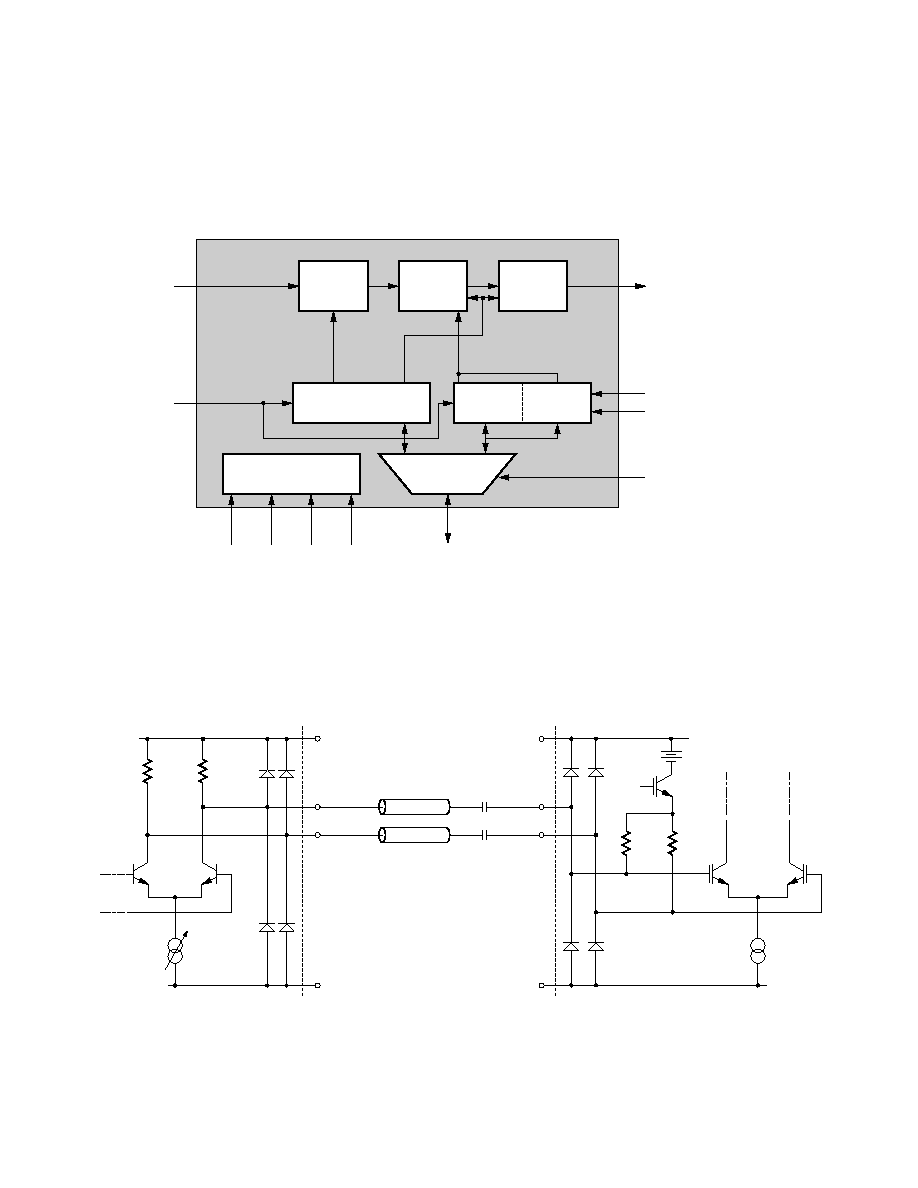
Block Description
Figure 1 gives an overall block
diagram for the HDMP-3268. The
operation of HDMP-3268 is
discussed below.
Figure 1. Block diagram for the HDMP-3268.
Figure 2. High-speed output and input simplified circuit schematics.
3
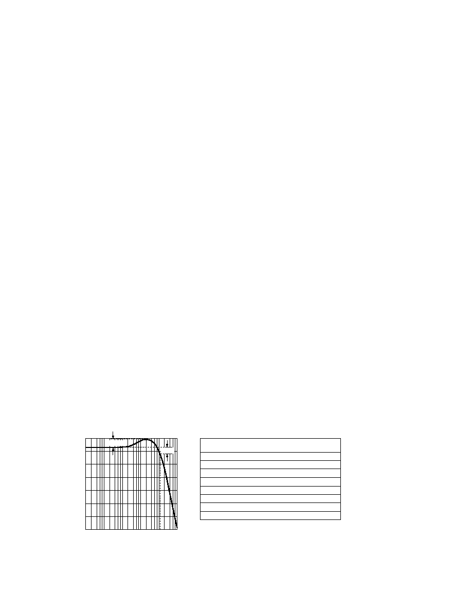
BOOST
3 dB
GAINDC
GAIN
FREQUENCY
Fpeak F3dB
HIGH SPEED INPUT
AC TRANSFER CHARACTERISTIC
TYPICAL PERFORMANCE OF HIGH SPEED
INPUT CELL WITH DIFFERENT EQUALIZATION SETTINGS
EQUALIZATION
SETTING
GAINDC
(dB)
BOOST
(dB)
Fpeak
(GHz)
F3dB
(GHz)
000
001
010
011
100
101
110
111
16.0
11.4
12.9
12.9
12.9
12.9
10.5
9.8
0
3.7
4.8
5.4
5.8
6.1
6.5
7.3
N/A
3.4
2.7
2.3
2.0
1.8
1.8
1.8
7.9
10.7
10.2
10.0
9.8
9.8
10.6
11.2
THIS DATA IS FOR ILLUSTRATIVE PURPOSES ONLY.
High-Speed Inputs and Outputs
Figure 2 shows simplified circuit
diagrams for the HDMP-3268's
high speed input and output cells.
A typical connection between the
output and input cells is also
shown. The output cell is
designed to drive 50
transmis-
sion lines and to be terminated at
the destination end in 50
.
When the output is intended to
connect to the input of another
HDMP-3268 as in a CLOS
architecture, no AC coupling
capacitors are required. The
output amplitude of the HDMP-
3268 is programmable in three
levels from approximately
500 mV to 1.0 V peak-to-peak
differential. In addition, the
output driver and its associated
multiplexer can be turned off to
save power if an output is not
used.
The HDMP-3268 high speed
input cell provides on-chip
termination resistors of 50
from each input to an on-chip
bias voltage generator which sets
the input common mode voltage
at approximately 0.7 V below the
positive supply. When the input is
intended to be DC coupled, as in
the case of the input being
connected to the output of
another HDMP-3268, the
common mode bias voltage is
disconnected from the termina-
tion resistors, and the two 50
resistors form a 100
differential termination. DC
coupling is the default setting for
the HDMP-3268. The input cell
has levels of input equalization
which can be programmed
through the digital control
interface. The AC termination
voltage also can be enabled
through a control register.
Unused input cells can be
disabled to save power.
Figure 3 shows a typical transfer
characteristic of the high-speed
input for the different input
equalization settings. The correct
equalization setting depends
upon the actual PCB environment
in which the HDMP-3268 resides.
The recommended procedure to
set the input equalization setting
is to characterize the HDMP-3268
on the PCB and to adjust the
equalization setting to give
minimum jitter at the output of
the HDMP-3268. The correct
equalization settings should be
stored and loaded into the
HDMP-3268 upon power-up. The
AC characteristics of the high
speed input, high speed output,
and multiplexer block are
specified in Table 8, AC Electrical
Specifications.
Digital Interface
The HDMP-3268 has a parallel bi-
directional digital interface for
configuring the switch matrix and
for controlling the various
functions such as input
equalization, output amplitude,
and power on/off. All of the
registers can be read back to
check valid programming. There
are 204 7-bit registers organized
into three sets of 68 registers
each. One set is used to control
power on/off, equalization, etc.
The other two sets are used to
configure the switch matrix. The
individual registers are accessed
using an address/data scheme.
The particular register address is
placed on the CH[6:0] lines, and
the register data is placed on the
DATA[6:0] lines, either by the
controller in write mode (RW=0),
or by the HDMP-3268 in read
mode (RW=1). Data is latched
into the internal registers on the
rising edge of WSTB. The control
registers are accessed when the
CNTL signal is high. Otherwise,
the address registers are
accessed. Figure 4 and Table 1
show the register read and write
timing diagram and specifica-
tions. See the switch matrix
configuration section for more
details. A chip select signal allows
Figure 3. Typical high-speed input equalization curve.
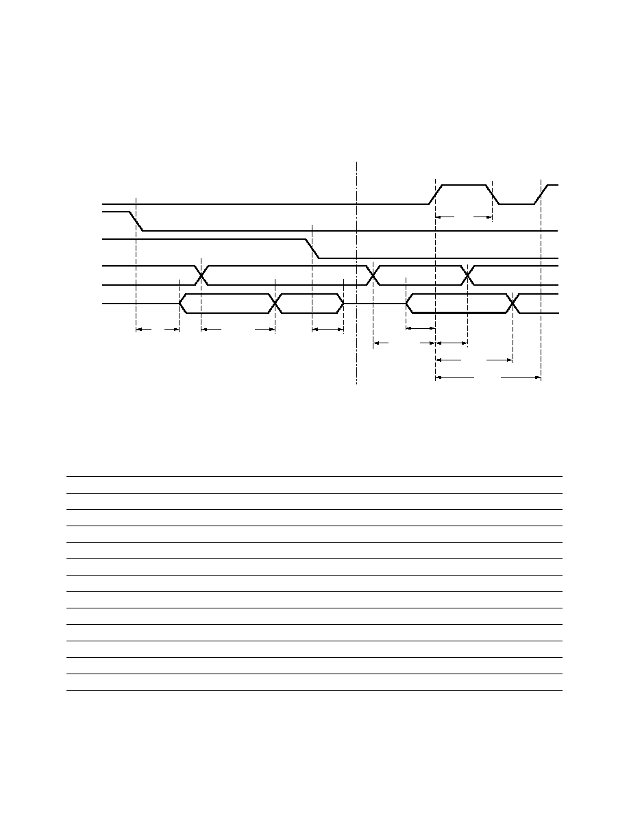
4
READ MODE
WRITE MODE
tpw
tcs
tDaccess
tWHiZ
tDsetup
tCsetup
tCHsetup
tChold
tCHhold
tDhold
tperiod
WSTB
CS
PW
CH[6:0]
SET CNTL
DATA[6:0]
multiple HDMP-3268s to reside
on the same address and data
buses. When CS is high, the
HDMP-3268 does not accept
data, and the HDMP-3268's data
outputs are tri-stated. In
Figure 4. Timing diagram for accessing HDMP-3268 registers.
Table 1. HDMP-3268 Interface Timing Requirements
T
A
= 0
∞
C to T
C
= 85
∞
C, V
CC
= V
DD
= V
CC
_DOUT = 2.35 V to 2.65 V
Symbol
Parameter
Units
Min.
Typ.
Max.
t
period
Write Strobe Period
ns
15.2
t
pw
Write Strobe Pulse Width
ns
3
0.6* t
period
t
rise/fall
Write Strobe Rise and Fall Times
ns
2
t
Dsetup
Data Setup Time
ns
2
1
t
Dhold
Data Hold Time
ns
0.5
0
t
CHsetup
Channel Setup Time
ns
8
t
CHhold
Channel Hold Time
ns
1
t
Csetup
Control Setup Time
ns
4
3
t
Chold
Control Hold Time
ns
≠0.7
≠1.2
t
cs
Chip Select to Data Out
ns
5
7.4
t
Daccess
Data Access Time
ns
10
13
t
WHiZ
Write Assert to High Z Time
ns
3
4
broadcast write mode, (CH[6:0]
set to `1111111'), all registers of
the selected set (control or
address) receive the same data
value. This feature simplifies chip
configuration upon power-up. By
default, all registers are
programmed to 0 at power-up
provided V
CC
comes up at the
same time or after V
DD
.

5
Table 2. HDMP-3268 Control Register Definition
Bit(s)
Name
Value
Definition
6:5
Output On/Off & Amplitude
[1]
00
Output stage disabled (power off)
01
Typical Vop
[1]
= 550 mV
10
Typical Vop
[1]
= 800 mV
11
Typical Vop
[1]
= 1050 mV
4:2
Equalization Amplitude
000
Input equalization disabled
111
Maximum input equalization
1
Input On/Off
0
Input stage disabled (power off)
1
Input stage active (power on)
0
AC/DC
0
DC input coupling
1
AC input coupling
Note:
1. Output Peak-to-Peak Differential Voltage, Vop, is specified as DOUT+ minus DOUT-. This measurement is made using a repeating 1010 pattern
with a 100
termination resistor across the DOUT+ and DOUT- outputs. The swing doubles if there is no termination resistor.
Control Register
The control register is used to
program the input AC or DC
coupling, input equalization,
output amplitude and power
on/off settings of each input and
output of the crosspoint switch.
To access the control register the
control signal CNTL must be
high. Table 2 gives the specific
Switch Matrix Configuration
The address registers are used to
program the connectivity of the
switch matrix. The address
registers are accessed when the
CNTL input is low. There are two
independent banks of 68 address
registers to allow one bank to be
programmed while the other bank
is controlling the switch matrix if
desired. There is one Address0
register and one Address1
register per output channel. The
address register selects the input
to be connected to its output.
Connecting a particular input to a
particular output is done by
setting CH[6:0] to the desired
Table 3. USE/SET Truth Table
Use
Set
Address Register Use
0
0
Using Address0 Registers for switch control, Reading/Writing Address0 Registers
0
1
Using Address0 Registers for switch control, Reading/Writing Address1 Registers
1
0
Using Address1 Registers for switch control, Reading/Writing Address0 Registers
1
1
Using Address1 Registers for switch control, Reading/Writing Address1 Registers
definition of each bit in the
control register. Upon power-up,
all bits of the control register are
set to 0.
output channel. DATA[6:0] holds
the channel number of the
desired input channel. Table 3
summarizes the behavior of the
USE and SET bits. See Figure 4
for the timing diagram for SET,
and Figure 5 for the timing
diagram for USE.