 | –≠–ª–µ–∫—Ç—Ä–æ–Ω–Ω—ã–π –∫–æ–º–ø–æ–Ω–µ–Ω—Ç: HDSP-0761 | –°–∫–∞—á–∞—Ç—å:  PDF PDF  ZIP ZIP |
Hexadecimal and Numeric
Displays for Industrial
Applications
Technical Data
Features
∑ Three Colors
High-Efficiency Red
Yellow
High Performance Green
∑ Two High-Efficiency Red
Options
Low Power
High Brightness
∑ Three Character Options
Numeric
Hexadecimal
Over Range
∑ Performance Guaranteed over
Temperature
∑ Memory Latch/Decoder/
Driver
TTL Compatible
∑ 4 x 7 Dot Matrix Character
∑ Categorized for Luminous
Intensity
∑ Yellow and Green
Categorized for Color
Typical Applications
∑ Industrial Equipment
∑ Computer Peripherals
∑ Instrumentation
∑ Telecommunication
Equipment
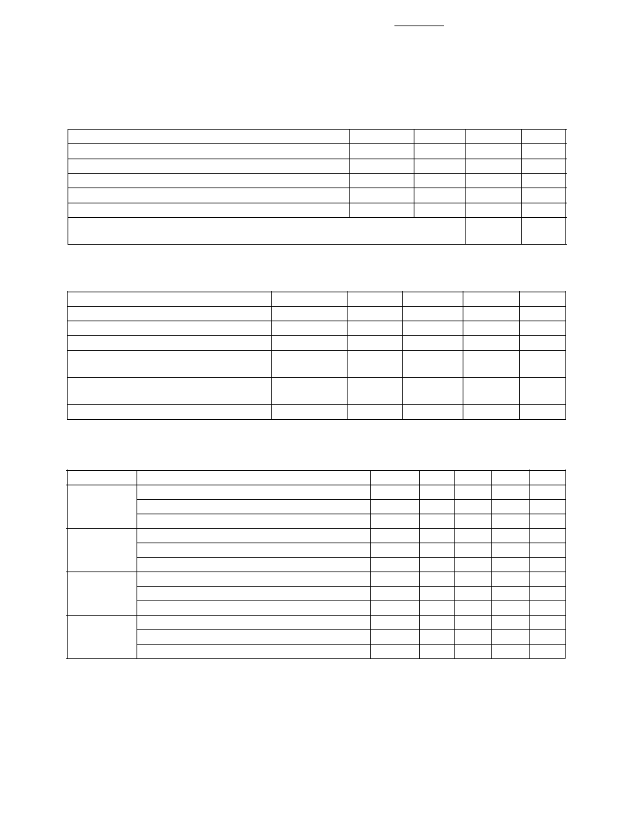
Device Selection Guide
Part Number
Front
HDSP-
Color
Description
View
0760
High-Efficiency
Numeric, Right Hand DP
A
0761
Red
Numeric, Left Hand DP
B
0762
Low Power
Hexadecimal
C
0763
Over Range
±
1
D
0770
High-Efficiency
Numeric, Right Hand DP
A
0771
Red
Numeric, Left Hand DP
B
0772
High Brightness
Hexadecimal
C
0763
Over Range
±
1
D
0860
Yellow
Numeric, Right Hand DP
A
0861
Numeric, Left Hand DP
B
0862
Hexadecimal
C
0863
Over Range
±
1
D
0960
Green
Numeric, Right Hand DP
A
0961
Numeric, Left Hand DP
B
0962
Hexadecimal
C
0963
Over Range
±
1
D
Description
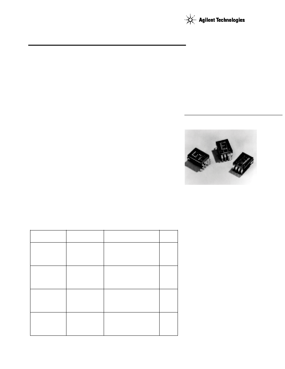
These solid state display devices
are designed and tested for use in
adverse industrial environments.
The character height is 7.4 mm
(0.29 inch). The numeric and
hexadecimal devices incorporate
an on-board IC that contains the
data memory, decoder and display
driver functions.
The numeric devices decode
positive BCD logic into characters
"0-9", a "≠" sign, decimal point,
and a test pattern. The hexadeci-
mal devices decode positive BCD
logic into 16 characters, "0-9, A-F."
An input is provided on the hexa-
decimal devices to blank the
display (all LEDs off) without
losing the contents of the memory.
The over range device displays
"
±
1" and right hand decimal point
and is typically driven via external
switching transistors.
HDSP-076x Series
HDSP-077x Series
HDSP-086x Series
HDSP-096x Series
2
Package Dimensions
Figure 2. Logic Block Diagram.
Figure 1. Timing Diagram
Z
3
Absolute Maximum Ratings
Description
Symbol
Min.
Max.
Unit
Storage Temperature, Ambient
T
S
-65
+100
∞
C
Operating Temperature, Ambient
[1]
T
A
-55
+85
∞
C
Supply Voltage
[2]
V
CC
-0.5
+7.0
V
Voltage Applied to Input Logic, dp and Enable Pins
V
I
, V
DP
, V
E
-0.5
V
CC
V
Voltage Applied to Blanking Input
[2]
V
B
-0.5
V
CC
V
Wave Solder Temperature at 1.59 mm (0.063 inch)
250
∞
C
below Body, max. 3 seconds
Recommended Operating Conditions
Description
Symbol
Min.
Nom.
Max.
Unit
Supply Voltage
[2]
V
CC
4.5
5.0
5.5
V
Operating Temperature, Ambient
[1]
T
A
-55
+85
∞
C
Enable Pulse Width
t
W
100
nsec
Time Data Must Be Held Before Positive
t
SETUP
50
nsec
Transition of Enable Line
Time Data Must Be Held After Positive
t
HOLD
50
nsec
Transition of Enable Line
Enable Pulse Rise Time
t
TLH
1.0
msec
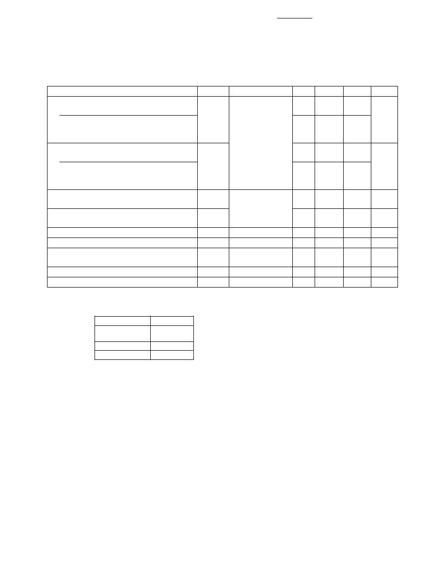
Optical Characteristics at
T
A
= 25
∞
C, V
CC
= 5.0 V
Device
Description
Symbol
Min.
Typ.
Max.
Unit
HDSP-0760
Luminous Intensity per LED (Digit Average)
[3,4]
I
V
65
140
µ
cd
Peak Wavelength
PEAK
635
nm
Dominant Wavelength
[5]
d
626
nm
HDSP-0770
Luminous Intensity per LED (Digit Average)
[3,4]
I
V
260
620
µ
cd
Peak Wavelength
PEAK
635
nm
Dominant Wavelength
[5]
d
626
nm
HDSP-0860
Luminous Intensity per LED (Digit Average)
[3,4]
I
V
215
490
µ
cd
Peak Wavelength
PEAK
583
nm
Dominant Wavelength
[5,6]
d
585
nm
HDSP-0960
Luminous Intensity per LED (Digit Average)
[3,4]
I
V
298
1100
µ
cd
Peak Wavelength
PEAK
568
nm
Dominant Wavelength
[5,6]
d
574
nm
Notes:
1. The nominal thermal resistance of a display mounted in a socket that is soldered onto a printed circuit board is R
JA
= 50
∞
C/W/
device. The device package thermal resistance is R
J-PIN
= 15
∞
C/ W/device. The thermal resistance device pin-to-ambient through
the PC board should not exceed 35
∞
C/W/device for operation at T
A
= +85
∞
C.
2. Voltage values are with respect to device ground, pin 6.
3. These displays are categorized for luminous intensity with the intensity category designated by a letter code located on the back of
the display package. Case temperature of the device immediately prior to the light measurement is equal to 25
∞
C.
Series
Series
Series
Series
4
Electrical Characteristics;
T
A
= -55
∞
C to +85
∞
C
Description
Symbol
Test Conditions
Min. Typ.
[7]
Max.
Unit
Supply Current
HDSP-0760 Series
I
CC
V
CC
= 5.5 V
78
105
mA
HDSP-0770 Series
120
175
HDSP-0860 Series
HDSP-0960 Series
Power Dissipation
HDSP-0760 Series
P
T
390
573
mW
HDSP-0770 Series
690
963
HDSP-0860 Series
HDSP-0960 Series
Logic, Enable and Blanking Low-Level Input
V
IL
V
CC
= 4.5 V
0.8
V
Voltage
Logic, Enable and Blanking High-Level
V
IH
2.0
V
Input Voltage
Logic and Enable Low-Level Input Current
I
IL
V
CC
= 5.5 V
-1.6
mA
Blanking Low-Level Input Current
I
BL
V
IL
= 0.4 V
-10
µ
A
Logic, Enable and Blanking High-Level
I
IH
V
CC
= 5.5 V
+40
µ
A
Input Current
V
IH
= 2.4 V
Weight
1.0
gm
Leak Rate
5x10
-8
cc/sec
Notes:
4. The luminous intensity at a specific operating ambient temperature, I
V
(T
A
) may be approximated from the following exponential
equation: I
V
(T
A
= I
V
(25
∞
C) e
[k (T - 25
∞
C)]
.
Device
K
HDSP-0760 Series
-0.0131/
∞
C
HDSP-0770 Series
HDSP-0860 Series
-0.0112/
∞
C
HDSP-0960 Series
-0.0104/
∞
C
5. The dominant wavelength,
d
, is derived from the CIE Chromaticity Diagram and is that single wavelength which defines the color of the
device.
6. The HDSP-0860 and HDSP-0960 series devices are categorized as to dominant wavelength with the category designated by a number on
the back of the display package.
7. All typical values at V
CC
= 5.0 V and T
A
= 25
∞
C.
(Characters "5."
or "B" Displayed)
A
5
Operational
Considerations
Electrical
These devices use a modified
4 x 7 dot matrix light emitting
diode to display decimal/hexa-
decimal numeric information. The
high efficiency red and yellow
LEDs are GaAsP epitaxial layer
on a GaP transparent substrate.
The green LEDs are GaP epitaxial
layer on a GaP transparent
substrate. The LEDs are driven
by constant current drivers, BCD
information is accepted by the
display memory when the enable
line is at logic low and the data is
latched when the enable is at
logic high. Using the enable pulse
width and data setup and hold
times listed in the Recommended
Operating Conditions allows data
to be clocked into an array of
displays at a 6.7 MHz rate.
The decimal point input is active
low true and this data is latched
into the display memory in the
same fashion as the BCD data.
The decimal point LED is driven
by the on-board IC.
The blanking control input on the
hexadecimal displays blanks (turns
off) the displayed information
without disturbing the contents of
display memory. The display is
blanked at a minimum threshold
level of 2.0 volts. When blanked,
the display standby power is
nominally 250 mW at T
A
= 25
∞
C.
Mechanical
The primary thermal path for
power dissipation is through the
device leads. Therefore, to insure
reliable operation up to an
ambient temperature of +85
∞
C, it
is important to maintain a case-
to-ambient thermal resistance of
less than 35
∞
C watt/device as
measured on top of display pin 3.
For information on soldering and
post solder cleaning see Applica-
tion Note 1027, Soldering LED
Components
.
Contrast Enhancement
These display devices are
designed to provide an optimum
ON/OFF contrast when placed
behind an appropriate contrast
enhancement filter. For further
information, please refer to
Application Note 1015, Contrast
Enhancement Techniques for
LED Displays.
Over Range Display
The over range devices display
"
±
1" and decimal point. The
character height and package
configuration are the same as the
numeric and hexadecimal
devices. Character selection is
obtained via external switching
transistors and current limiting
resistors.
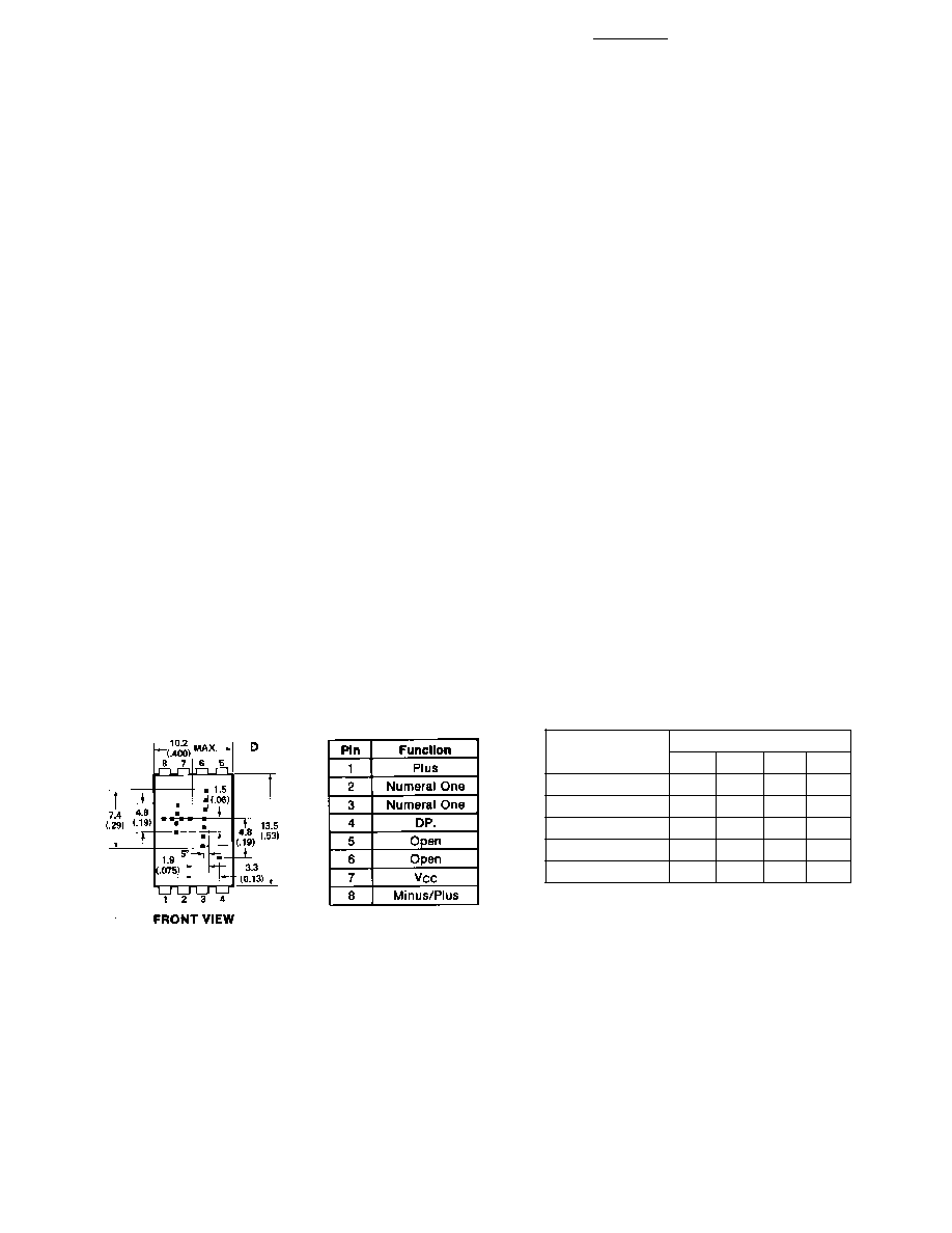
NOTE: 1. DIMENSIONS IN MILLIMETRES AND (INCHES).
Package Dimensions
Pin
Character
1
2,3
4
8
+
1
X
X
1
-
0
X
X
1
1
X
1
X
X
Decimal Point
X
X
1
X
Blank
0
0
0
0
Notes:
0: Line switching transistor in Figure 7 cutoff.
1: Line switching transistor in Figure 7 saturated.
X: 'don't care'