 | –≠–ª–µ–∫—Ç—Ä–æ–Ω–Ω—ã–π –∫–æ–º–ø–æ–Ω–µ–Ω—Ç: HDSP-2301 | –°–∫–∞—á–∞—Ç—å:  PDF PDF  ZIP ZIP |
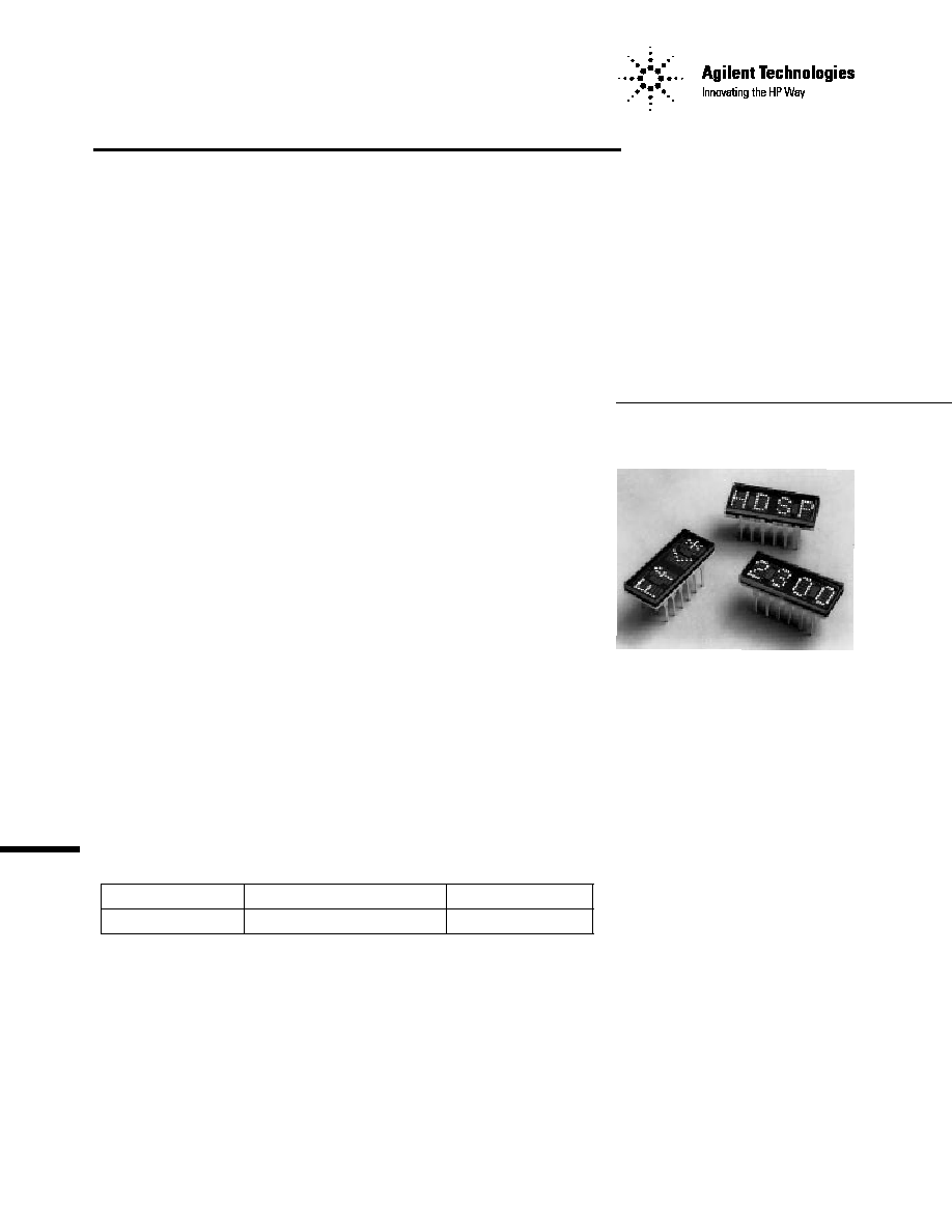
Four Character 5.0 mm (0.20 inch)
5 x 7 Alphanumeric Displays
HDSP-2301
HDSP-2302
HDSP-2303
Technical Data
Features
∑ Integrated Shift Registers
with Constant Current
Drivers
∑ Compact Ceramic Package
∑ Wide Viewing Angle
∑ End Stackable Four
Character Package
∑ TTL Compatible
∑ 5 x 7 LED Matrix Displays
Full ASCII Set
∑ Categorized for Luminous
Intensity
∑ HDSP-2301/2303
Categorized for Color
Applications
∑ Avionics
∑ Business Machines
∑ Medical Instruments
∑ Portable Data Entry Devices
Description
The HDSP-2301/-2302/-2303
series of displays are
5.0 mm (0.20 inch) 5 x 7 LED
arrays for display of alpha-
numeric information. These
devices are available in yellow,
high efficiency red, and high
performance green. Each four
character cluster is contained in a
12 pin dual-in-line package. An
Devices
Yellow
High Efficiency Red
Green
HDSP-2301
HDSP-2302
HDSP-2303
on-board SIPO (Serial-In-Parallel-
Out) 7-bit shift register
associated with each digit
controls constant current LED
row drivers. Full character
display is achieved by external
column strobing.
2
Absolute Maximum Ratings
(HDSP-2301/-2302/-2303)
Supply Voltage, V
CC
to Ground ...................................... ≠0.5 V to 6.0 V
Inputs, Data Out and V
B
.................................................. ≠0.5 V to V
CC
Column Input Voltage, V
COL
....................................... ≠0.5 V to +6.0 V
Free Air Operating Temperature Range, T
A
[1,2]
.......... ≠20∞C to +85∞C
Storage Temperature Range, T
S
................................ ≠55∞C to +100∞C
Maximum Allowable Package Dissipation at T
A
= 25∞C
[1,2,3]
HDSP-2301/-2302/-2303 .................................................. 1.46 Watts
Maximum Solder Temperature 1.59 mm (0.63")
Below Seating Plane t < 5 sec ................................................. 260∞C
Recommended Operating Conditions (HDSP-2301/-2302/-2303)
Parameter
Symbol
Min.
Nom. Max. Units Fig.
Supply Voltage
V
CC
4.75
5.0
5.25
V
Data Out Current, Low State
I
OL
1.6
mA
Data Out Current, High State
I
OH
≠0.5
mA
Column Input Voltage, Column On HDSP-2301/-2302/-2303
V
COL
2.75
3.5
V
4
Setup Time
t
setup
70
45
ns
1
Hold Time
t
hold
30
0
ns
1
Width of Clock
t
w(Clock)
75
ns
1
Clock Frequency
f
clock
0
3
MHz
1
Clock Transition Time
t
THL
200
ns
1
Free Air Operating Temperature Range
[1,2]
T
A
≠20
85
∞C
2
Package Dimensions
20.01
(0.790)
MAX.
2.84
(0.112)
REF.
SEE NOTE 3
SEE
NOTE 3
8.43
(0.335)
4.87
(0.192) REF.
5.00 ± 0.13
(0.197 ± 0.005)
1
2
3
4
5
6
12
11
10
9
8
7
PIN 1 MARKED BY DOT
ON BACK OF PACKAGE
5.08
(0.200)
2.54
(0.100)
1.27 ± 0.13
(0.050 ± 0.005)
6.85 (0.270)
2.54 ± 0.13
(0.100 ± 0.005)
NON ACCUM.
TYP.
1.27
(0.050)
TYP.
0.54 ± 0.08
(0.020 ± 0.003)
C
L
6.35 ± 0.25
(0.250 ± 0.010)
0.25 ± 0.05
(0.010 ± 0.002)
TYP.
PIN
FUNCTION
PIN
FUNCTION
1
2
3
4
5
6
COLUMN 1
COLUMN 2
COLUMN 3
COLUMN 4
COLUMN 5
INT. CONNECT*
7
8
9
10
11
12
DATA OUT
VB
VCC
CLOCK
GROUND
DATA IN
*DO NOT CONNECT OR USE
NOTES:
1. DIMENSIONS IN MILLIMETERS (INCHES).
2. UNLESS OTHERWISE SPECIFIED, THE TOLERANCE
ON ALL DIMENSIONS IS ± 0.38 mm (± 0.015").
3. CHARACTERS ARE CENTERED WITH RESPECT TO
LEADS WITHIN ± 0.13 mm (± 0.005").
1
2
3
4
MAX.
3
Electrical Characteristics over Operating Temperature Range
(Unless otherwise specified)
*All typical values specified at V
CC
= 5.0 V and T
A
= 25∞C unless otherwise noted.
**Power dissipation per package with four characters illuminated.
Notes:
1. Operation above 85∞C ambient is possible provided the following conditions are met. The junction temperature should not exceed 125∞C
T
J
and the case temperature (as measured at pin 1 or the back of the display) should not exceed 100∞C T
C
.
2. The HDSP-2301/-2302/-2303 should be derated linearly above 37∞C at 16.7 mW/∞C. This derating is based on a device mounted in a
socket having a thermal resistance from case to ambient at 35∞** C/W per device. See Figure 2 for power deratings based on a lower
thermal resistance.
3. Maximum allowable dissipation is derived from V
CC
= 5.25 V, V
B
= 2.4 V, V
COL
= 3.5 V 20 LEDs on per character, 20% DF.
Supply Current
Column Current at any
Column Input
Column Current at any
Column Input
V
B
, Clock or Data Input
Threshold High
V
B
, Clock or Data Input
Threshold Low
Input Current
Logical 1
Input Current
Logical 0
Data Out Voltage
Power Dissipation Per
Package**
Thermal Resistance IC
Junction-to-Case
V
B
= 0.4 V
45
60
mA
V
B
= 2.4 V
73
95
mA
V
B
= 0.4 V
500
µ
A
V
B
= 2.4 V
380
520
mA
2.0
V
0.8
V
20
80
µ
A
10
40
µ
A
≠500
≠800
µ
A
≠250
≠400
µ
A
2.4
3.4
V
0.2
0.4
V
0.78
W
25
V
CC
= 5.25 V
V
CLOCK
= V
DATA
= 2.4 V
All SR Stages =
Logical 1
V
CC
= 5.25 V
V
COL
= 3.5 V
All SR Stages =
Logical 1
V
CC
= V
COL
= 4.75 V
V
CC
= 5.25 V, V
IH
= 2.4 V
V
CC
= 5.25 V, V
IL
= 0.4V
V
CC
= 4.75 V, I
OH
= ≠0.5 mA,
I
COL
= 0 mA
V
CC
= 4.75 V, I
OL
= 1.6 mA,
I
COL
= 0 mA
V
CC
= 5.0 V, V
COL
= 3.5 V,
17.5% DF
15 LEDs on per character,
V
B
= 2.4 V
Yellow HDSP-2301/High Efficiency Red HDSP-2302/ High Performance Green
HDSP-2303
I
CC
I
COL
I
COL
V
IH
V
IL
I
IH
I
IH
I
IL
I
IL
V
OH
V
OL
P
D
R
J≠C
Description
Symbol
Test Conditions
Min. Typ.* Max.
Units
Fig.
V
B
, Clock
Data In
V
B
, Clock
Data In
∞C/W/
Device
2
2
4
4
High Performance Green HDSP-2303
Description
Symbol
Test Conditions
Min. Typ.* Max. Units Fig.
Peak Luminous Intensity
I
vPeak
V
CC
= 5.0 V, V
COL
= 3.5 V 1280 2410
µ
cd
3
per LED
[4,8]
T
i
= 25∞C
[6]
, V
B
= 2.4 V
(Character Average)
Peak Wavelength
PEAK
568
nm
Dominant Wavelength
[5,7]
d
574
nm
Yellow HDSP-2301
Description
Symbol
Test Conditions
Min. Typ.* Max. Units Fig.
Peak Luminous Intensity
I
vPeak
V
CC
= 5.0 V, V
COL
= 3.5 V
650
1140
µ
cd
3
per LED
[4,8]
T
i
= 25∞C
[6]
, V
B
= 2.4 V
(Character Average)
Peak Wavelength
PEAK
583
nm
Dominant Wavelength
[5,7]
d
585
nm
Optical Characteristics
High Efficiency Red HDSP-2302
Description
Symbol
Test Conditions
Min. Typ.* Max. Units Fig.
Peak Luminous Intensity
I
vPeak
V
CC
= 5.0 V, V
COL
= 3.5 V
650
1430
µ
cd
3
per LED
[4,8]
T
i
= 25∞C
[6]
, V
B
= 2.4 V
(Character Average)
Peak Wavelength
PEAK
635
nm
Dominant Wavelength
[7]
d
626
nm
*All typical values specified at V
CC
= 5.0 V and T
A
= 25∞C unless otherwise noted.
**Power dissipation per package with four characters illuminated.
Notes:
4. The characters are categorized for luminous intensity with the intensity category designated by a letter code on the bottom of
the package.
5. The HDSP-2301/-2303 are categorized for color with the color category designated by a number code on the bottom of
the package.
6. T
i
refers to the initial case temperature of the device immediately prior to the light measurement.
7. Dominant wavelength
d
, is derived from the CIE chromaticity diagram, and represents the single wavelength which defines
the color of the device.
8. The luminous sterance of the LED may be calculated using the following relationships:
L
v
(cd/m
2
) = l
v
(Candela)/A (Metre)
2
L
v
(Footlamberts) =
i
v
(Candela)/A (Foot)
2
A = 5.3 x 10
≠8
M
2
= 5.8 x 10
≠7
(Foot)
2
5
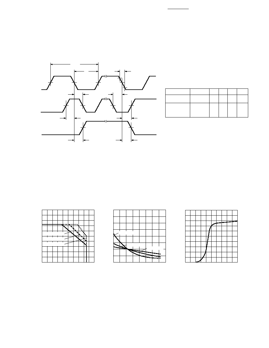
Figure 1. Switching Characteristics HDSP-2301/-2302/-2303 (T
A
= ≠20∞C to +85∞C).
Figure 3. Relative Luminous Intensity
vs. Temperature.
Figure 2. Maximum Allowable Power
Dissipation vs. Temperature.
Figure 4. Peak Column Current vs.
Column Voltage.
P
D MAX.
≠ MAXIMUM ALLOWABLE POWER
DISSIPATION ≠ WATTS
0
0
TA ≠ AMBIENT TEMPERATURE ≠ ∞C
90
20
70 80
100
2.0
1.8
1.6
1.4
1.0
0.8
0.4
0.2
60
50
40
30
10
R
JA
= 60∞C/W
R
JA
= 50∞C/W
R
JA
= 40∞C/W
1.2
0.6
RELATIVE LUMINOUS INTENSITY
0
TJ ≠ JUNCTION TEMPERATURE ≠ ∞C
120
4.0
60
0
20
80
140
3.0
2.0
1.0
-20
40
100
HDSP-2302
HDSP-2301
HDSP-2303
I COL
≠ PEAK COLUMN CURRENT ≠ mA
0
0
VCOL ≠ COLUMN VOLTAGE ≠ VOLTS
5.0
3.0
500
400
300
200
1.0
2.0
4.0
100
HDSP-2301/-2302/-2303
tHOLD
1/fMAX.
tW
tTHL
tSETUP
tSETUP
tHOLD
tPHL
tPLH
PARAMETER
CONDITION
MIN. TYP. MAX. UNITS
fCLOCK
CLOCK RATE
3
MHz
tPLH, tPHL
PROPAGATION
DELAY CLOCK
TO DATA OUT
CL = 15 pF
RL = 2.4 K
125
ns
CLOCK
DATA IN
DATA OUT
1.5 V
1.5 V
90 %
10 %
1.5 V
1.5 V
1.5 V
1.5 V
1.5 V
1.5 V
1.5 V
1.5 V
2.4 V
0.4 V
2.4 V
0.4 V
2.4 V
0.4 V