 | –≠–ª–µ–∫—Ç—Ä–æ–Ω–Ω—ã–π –∫–æ–º–ø–æ–Ω–µ–Ω—Ç: HDSP-2502 | –°–∫–∞—á–∞—Ç—å:  PDF PDF  ZIP ZIP |
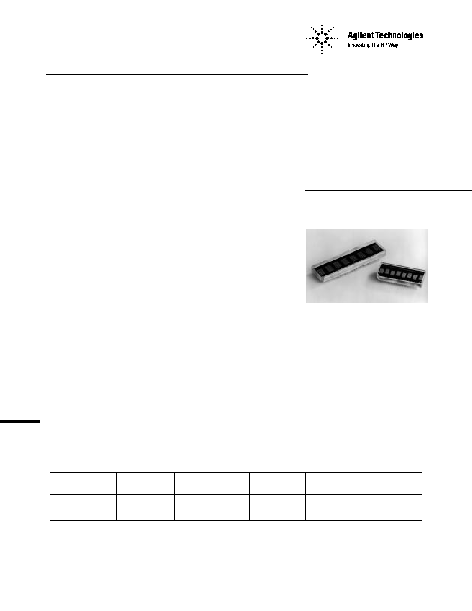
Eight Character 5 mm and 7 mm
Smart Alphanumeric Displays
Technical Data
Features
∑ X Stackable (HDSP-21XX)
∑ XY Stackable (HDSP-250X)
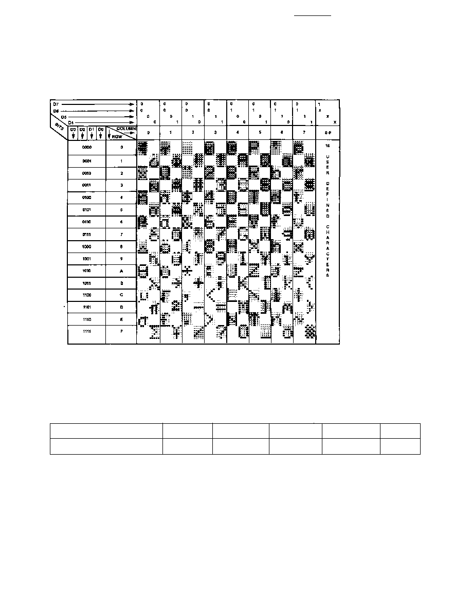
∑ 128 Character ASCII
Decoder
∑ Programmable Functions
∑ 16 User Definable
Characters
∑ Multi-Level Dimming and
Blanking
∑ TTL Compatible CMOS IC
∑ Wave Solderable
Applications
∑ Computer Peripherals
∑ Industrial Instrumentation
∑ Medical Equipment
∑ Portable Data Entry Devices
∑ Cellular Phones
∑ Telecommunications
Equipment
∑ Test Equipment
Description
The HDSP-210X/-211X/-250X
series of products is ideal for
applications where displaying
eight or more characters of dot
matrix information in an
aesthetically pleasing manner is
required. These devices are
8-digit, 5 x 7 dot matrix, alpha-
numeric displays and are all
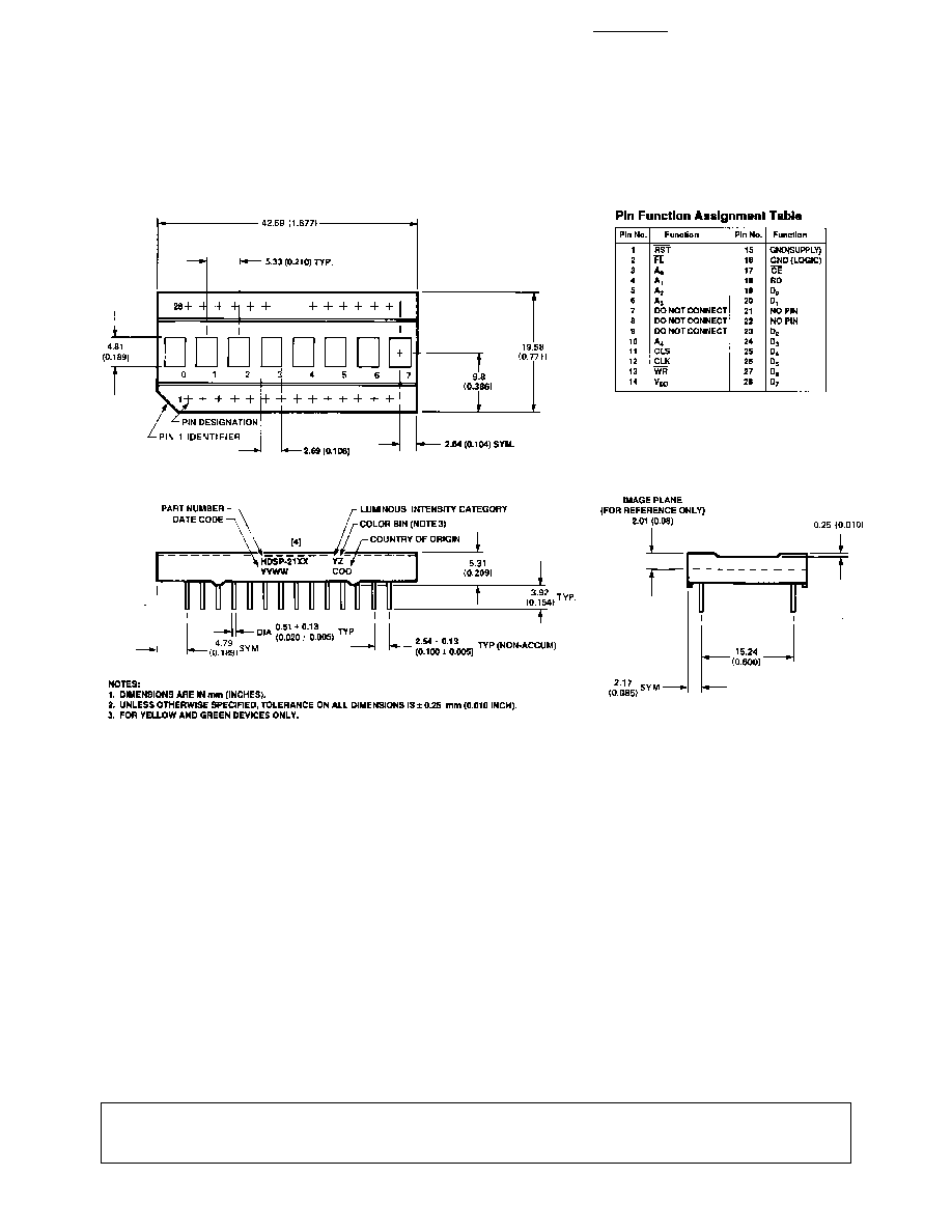
packaged in a standard 15.24 mm
(0.6 inch) 28 pin DIP. The on-
board CMOS IC has the ability to
decode 128 ASCII characters
which are permanently stored in
ROM. In addition, 16 program-
mable symbols may be stored in
on-board ROM, allowing consider-
HDSP-210X Series
HDSP-211X Series
HDSP-250X Series
able flexibility for displaying
additional symbols and icons.
Seven brightness levels provide
versatility in adjusting the display
intensity and power consumption.
The HDSP-210X/-211X/-250X
products are designed for
standard microprocessor interface
techniques. The display and
special features are accessed
through a bidirectional 8-bit data
bus.
Device Selection Guide
AlGaAs
High Efficiency
Font Height
Red
Red
Orange
Yellow
Green
0.2 inches
HDSP-2107
HDSP-2112
HDSP-2110
HDSP-2111
HDSP-2113
0.27 inches
HDSP-2504
HDSP-2502
HDSP-2500
HDSP-2501
HDSP-2503
2
Package Dimensions
ESD WARNING: STANDARD CMOS HANDLING PRECAUTIONS SHOULD BE OBSERVED TO AVOID
STATIC DISCHARGE.
Absolute Maximum Ratings
Supply Voltage, V
DD
to Ground
[1]
........................................ -0.3 to 7.0 V
Operating Voltage, V
DD
to Ground
[2]
.............................................. 5.5 V
Input Voltage, Any Pin to Ground .............................. -0.3 to V
DD
+0.3 V
Free Air Operating Temperature Range, T
A
[3]
................ - 45
∞
C to +85
∞
C
Storage Temperature Range, T
S
.................................. -55
∞
C to +100
∞
C
Relative Humidity (non-condensing) ............................................... 85%
Maximum Solder Temperature
(Below Seating Plane), t < 5 sec .............................................. 260
∞
C
ESD Protection @ 1.5 k
, 100 pF ........................ V
Z
= 4 kV (each pin)
Notes:
1. Maximum Voltage is with no LEDs illuminated.
2. 20 dots ON in all locations at full brightness.
3. Maximum supply voltage is 5.25 V for operation above 70
∞
C.

3
Package Dimensions
4
ASCII Character Set
HDSP-210X, HDSP-211X, HDSP-250X Series
Recommended Operating Conditions
Parameter
Symbol
Minimum
Nominal
Maximum
Units
Supply Voltage
V
DD
4.5
5.0
5.5
V
5
Electrical Characteristics Over Operating Temperature Range (-45
∞
C to +85
∞
C)
4.5 V < V
DD
< 5.5 V, unless otherwise specified
T
A
= 25
∞
C
-45
∞
C < T
A
< + 85
∞
C
V
DD
= 5.0 V
4.5 V < V
DD
< 5.5 V
Parameter
Symbol
Typ.
Max.
Min.
Max.
Units
Test Conditions
Input Leakage
I
IH
1.0
µ
A
V
IN
= 0 to V
DD
,
(Input without pullup)
I
IL
-1.0
pins CLK, D
0
-D
7
,
A
0
-A
4
Input Current
I
IPL
-11
-18
-30
µ
A
V
IN
= 0 to V
DD
,
(Input with pullup)
pins CLS, RST,
WR, RD, CE, FL
I
DD
Blank
I
DD
(BLK)
0.5
3.0
4.0
mA
V
IN
= V
DD
I
DD
8 digits
I
DD
(V)
200
255
330
mA
"V" on in all 8
12 dots/character
[1,2]
locations
I
DD
8 digits
I
DD
(#)
300
370
430
mA
"#" on in all
20 dots/character
[1,2,3, 4]
locations
Input Voltage High
V
IH
2.0
V
DD
V
+0.3
Input Voltage Low
V
IL
GND
0.8
V
-0.3 V
Output Voltage High
V
OH
2.4
V
V
DD
= 4.5 V,
I
OH
= -40
µ
A
Output Voltage Low
V
OL
0.4
V
V
DD
= 4.5 V,
D
0
-D
7
I
OL
= 1.6 mA
Output Voltage Low
V
OL
0.4
V
V
DD
= 4.5 V,
CLK
I
OL
= 40
µ
A
High Level Output
I
OH
-60
mA
V
DD
= 5.0 V
Current
Low Level Output
I
OL
50
mA
V
DD
= 5.0 V
Current
Thermal Resistance
R
J-C
15
∞
C/W
IC Junction-to-Case
Notes:
1. Average I
DD
measured at full brightness. See Table 2 in Control Word Section for I
DD
at lower brightness levels. Peak
I
DD
= 28/15 x I
DD
(#).
2. Maximum I
DD
occurs at -55
∞
C.
3. Maximum I
DD
(#) = 355 mA at V
DD
= 5.25 V and IC T
J
= 150
∞
C.
4. Maximum I
DD
(#) = 375 mA at V
DD
= 5.5 V and IC T
J
= 150
∞
C.