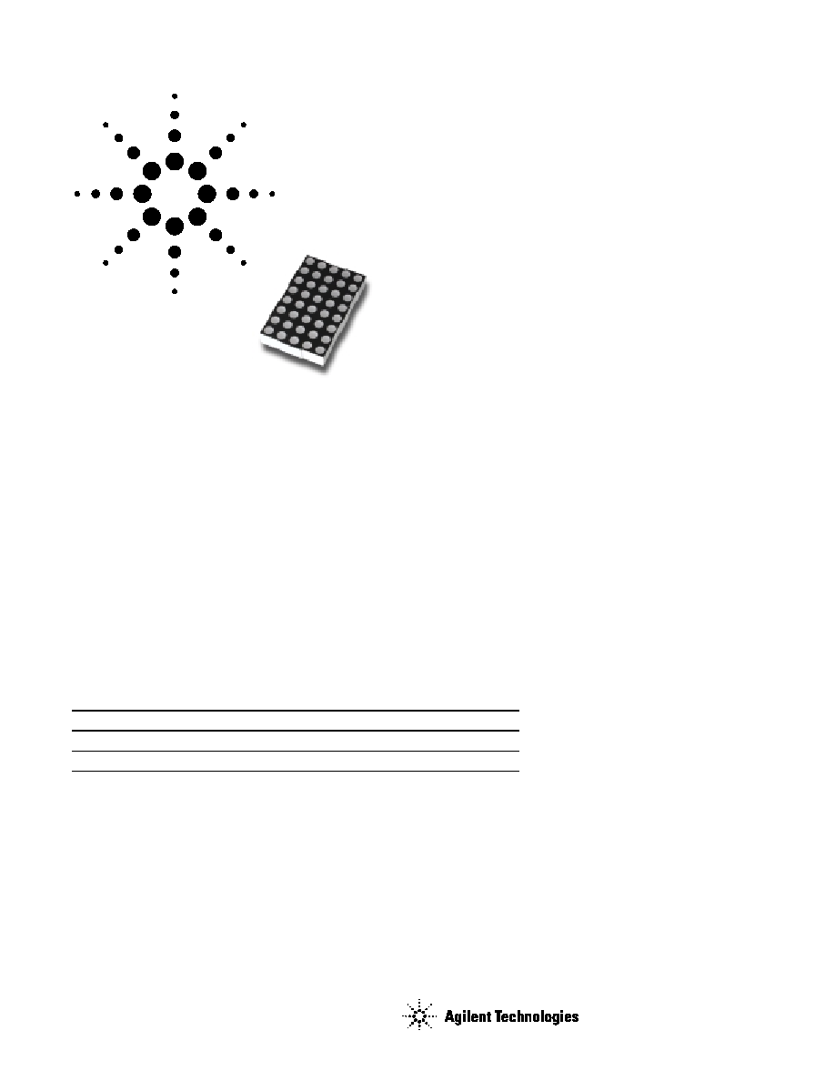
Agilent HDSP-B58x Series
53.3 mm (2.1 inch) General Purpose
5 x 8 Dot Matrix Bi-Color
Alphanumeric Displays
Data Sheet
Description
These displays have a 53.3 mm
(2.1 inch) character height. The
devices are available in either
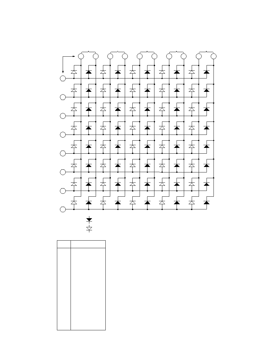
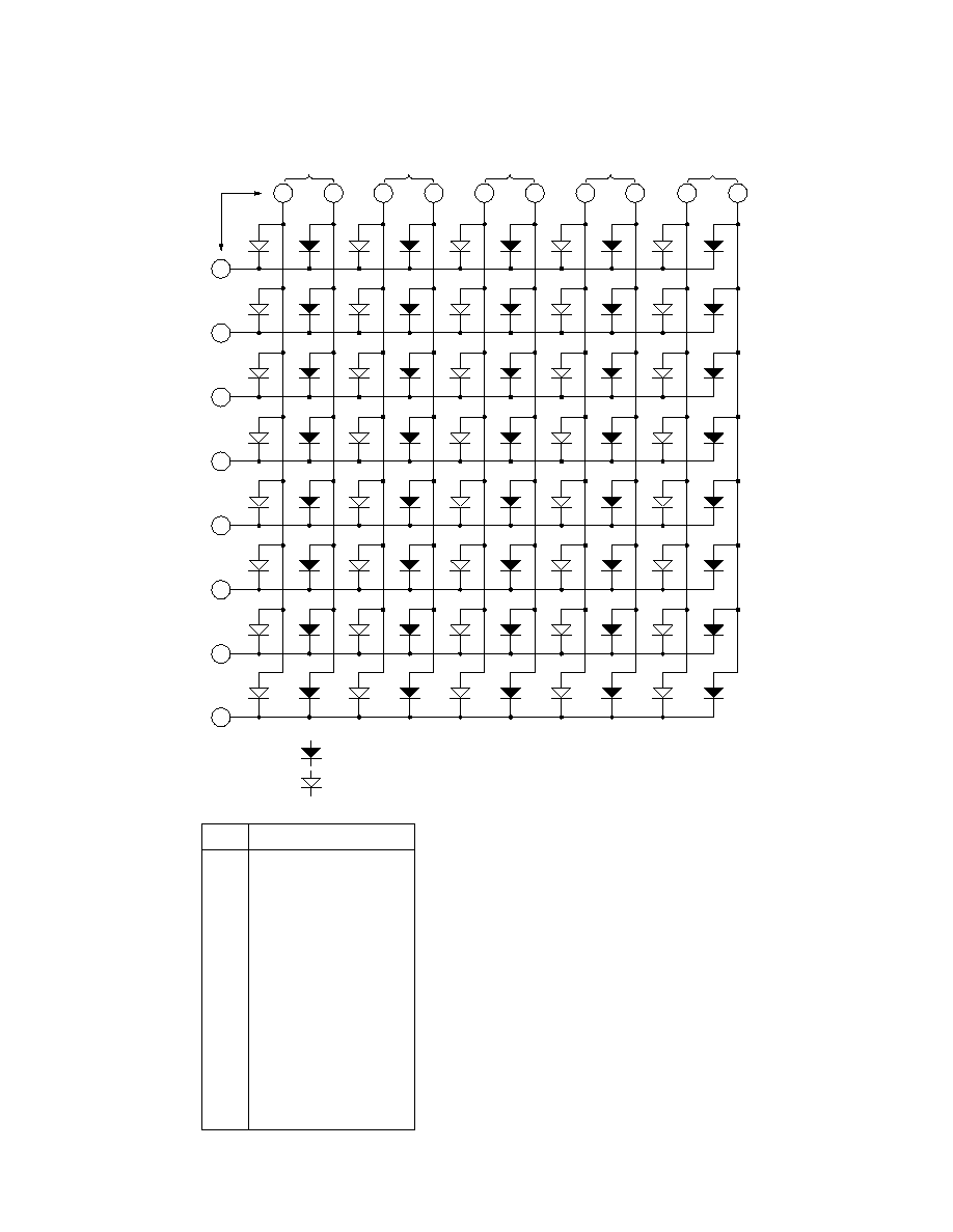
common row anode or common row
cathode configurations. The
displays come in only black face
paint. This bi-color display consists
of GaP Red (HER) and GaP Green
colors.
Features
∑ 5 x 8 Dot matrix font
∑ X-Y stackable
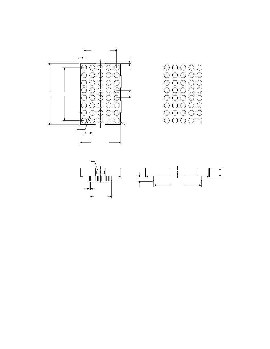
∑ Pin-out
≠ 45.72 mm (1.8 in.) Dual-In-Line
(DIP) leads on 2.54 mm (0.1 in.)
centers
∑ Color
≠ Bi-color: GaP Red and GaP Green
∑ Face paint color: black
∑ Design flexibility
≠ Common row anode or common
row cathode
∑ Categorized for luminance
Applications
∑ Suitable for indoor use
∑ Not recommended for industrial
applications, i.e., operating
temperature requirements
exceeding 85
∞
C or below ≠35
∞
C
∑ Extreme temperature cycling not
recommended
[1]
These parts are subjected to Out-
going Quality Assurance (OQA)
inspection with an AQL of
0.065% for functional and visual/
cosmetic defects.
Devices
HDSP-
Description
B581
53.3 mm Black Surface Common Row Anode
B582
53.3 mm Black Surface Common Row Cathode
Note:
1. For details, please contact your local Agilent components sales office or an authorized distributor.
5
Absolute Maximum Ratings at T
A
= 25∞C
GaP Red
GaP Green
Parameter
HDSP-B581/B582
HDSP-B581/B582
Units
Average Power per Dot
[1]
65
65
mW
Peak Forward Current per Dot
[1]
(1/8 Duty Cycle at 10 kHz)
80
100
mA
Average Forward Current per Dot
25
[1,2]
25
[1,3]
mA
Reverse Voltage per Dot
3
3
V
Operating Temperature
≠35 to +85
≠35 to +85
∞
C
Storage Temperature
≠35 to +85
≠35 to +85
∞
C
Wave Soldering Temperature for 3 seconds
[4]
(2 mm [0.078 in.] below Body)
250
250
∞
C
Notes:
1. Do not exceed maximum average current per dot.
2. Derate above 25
∞
C at 0.20 mA/
∞
C.
3. Derate above 25
∞
C at 0.33 mA/
∞
C.
4. Not recommended to be soldered more than two times. Minimum interval between solderings is 15 minutes.
Total soldering time not to exceed 3 seconds.