 | –≠–ª–µ–∫—Ç—Ä–æ–Ω–Ω—ã–π –∫–æ–º–ø–æ–Ω–µ–Ω—Ç: HEMT-3301 | –°–∫–∞—á–∞—Ç—å:  PDF PDF  ZIP ZIP |
940 nm High Radiant Emitters
Technical Data
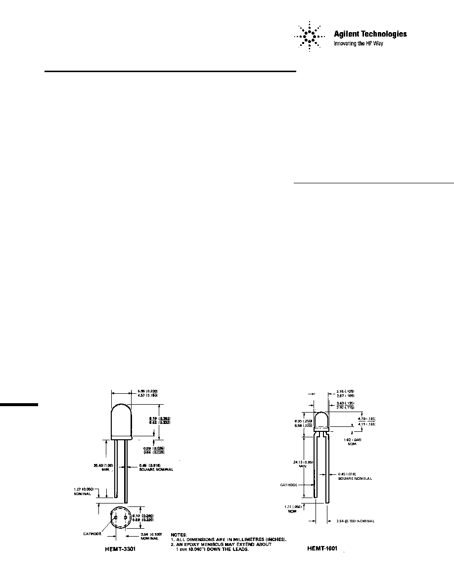
HEMT-3301
HEMT-1001
Features
∑ Nonsaturating, High Radiant
Flux Output
∑ Efficient at Low Currents,
Combined with High
Current Capability
∑ Three Package Styles
∑ Operating Temperature
Range -55
∞
C to +100
∞
C
∑ Medium-Wide Radiation
Patterns
∑ Radiated Spectrum Matches
Response of Silicon
Photodetectors
Description
The HEMT-3301 and HEMT-1001
are infrared emitters, using a
mesa structure GaAs on GaAs
infrared diode, IRED, optimized
for maximum quantum efficiency
at a peak wavelength of 940 nm.
The HEMT-3301 and HEMT-1001
emitters are untinted, undiffused
plastic packages with medium-
wide radiation patterns. These
Package Dimensions
medium-wide and wide radiation
patterns eliminate the beam
focusing problems that are
encountered with emitters that
have narrow radiation patterns.
Applications include optical
transducers, optical part
counters, smoke detectors, covert
identification, paper tape and
card readers, and optical
encoders.

2
Absolute Maximum Ratings at T
A
= 25
∞
C
Power Dissipation .................................................................... 150 mW
DC Forward Current .................................................................. 100 mA
(Derate as specified in Figure 6)
Peak Forward Current ............................................................. 1000 mA
(Time average current as determined from Figure 7)
IRED Junction Temperature ........................................................ 110
∞
C
Operating and Storage Temperature ........................... -55
∞
C to +100
∞
C
Lead Soldering Temperature .................................. 260
∞
C for 5 seconds
(1.6 mm (0.063 in.) from emitter body)
Electrical/Optical Characteristics at T
A
= 25
∞
C
Symbol
Description
Min.
Typ.
Max.
Units
Test Conditions
Fig.
I
e
Radiant Intensity
HEMT-3301
2.5
4.0
mW/sr
I
F
= 20 mA
4, 5
HEMT-1001
1.0
2.0
I
e
/
T
Temperature Coefficient
-0.58
%/
∞
C
Measured at
PEAK
1
for Radiant Intensity
[1]
/
T
Temperature Coefficient
0.3
nm/
∞
C
Measured at
PEAK
1
for Peak Wavelength
[2]
PEAK
Peak Wavelength
940
nm
Measured at
PEAK
1
2
1/2
Half Intensity
[3]
Total Angle
HEMT-3301
50
deg.
I
F
= 20 mA
8
HEMT-1001
60
9
t
r
Output Rise Time
1700
ns
I
PEAK
= 20 mA
(10% to 90%)
t
f
Output Fall Time
700
ns
I
PEAK
= 20 mA
(90% to 10%)
C
Capacitance
30
pf
V
F
= 0; f = 1 MHz
V
R
Reverse Breakdown
5.0
V
I
R
= 10
µ
A
Voltage
V
F
Forward Voltage
1.30
1.50
V
I
F
= 100 mA
2
1.15
I
F
= 20 mA
R
J-PIN
Thermal Resistance
HEMT-3301
260
∞
C/W
IRED Junction to
HEMT-1001
290
to Cathode Lead
Notes:
1. Radiant intensity at ambient temperature I
e
(T
A
) = I
e
(25
∞
C) + (
I
e
/
T) (T
A
- 25
∞
C)/100.
2. Peak wavelength at ambient temperature:
PEAK
(T
A
) =
PEAK
(25
∞
C) + (
/
T) (T
A
- 25
∞
C).
3.
1/2
is the off-axis angle from emitter centerline where the radiant intensity is half the on-axis value.
4. Approximate radiant flux output within a cone angle of 2
:
e
(2
) = [
e
(
)/I
e
(0)] I
e
(T
A
);
e
(
)/I
e
(0) obtained from Figure 8 or 9.
3
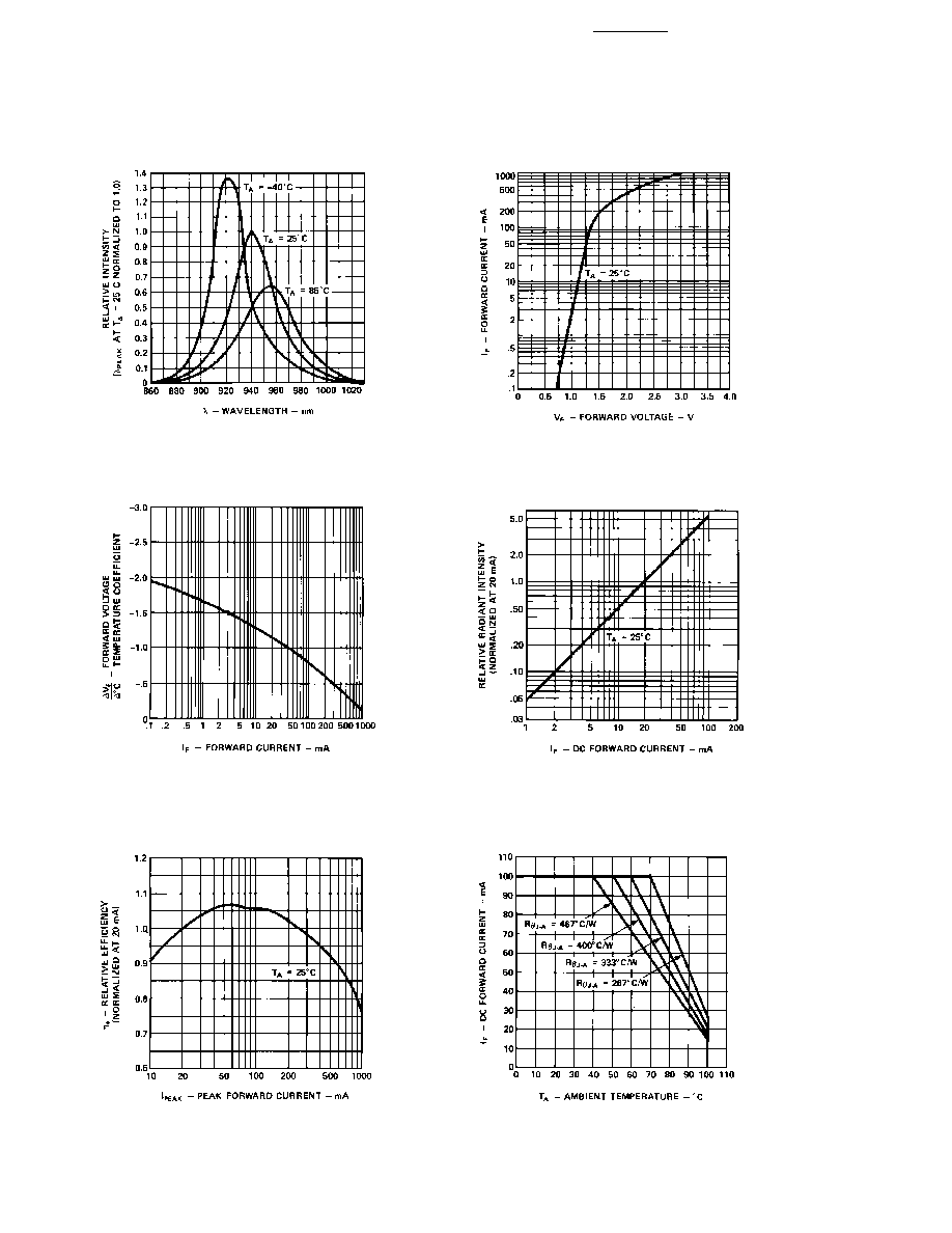
Figure 1. Radiated Spectrum.
Figure 2. Forward Current vs.
Forward Voltage.
Figure 5. Relative Efficiency vs. Peak
Forward Current.
Figure 6. Maximum DC Forward
Current vs. Ambient Temperature.
Derating Based on T
JMAX
= 110
∞
C.
Figure 3. Forward Voltage Tempera-
ture Coefficient vs. Forward Current.
Figure 4. Relative Radiant Intensity
vs. DC Forward Current.
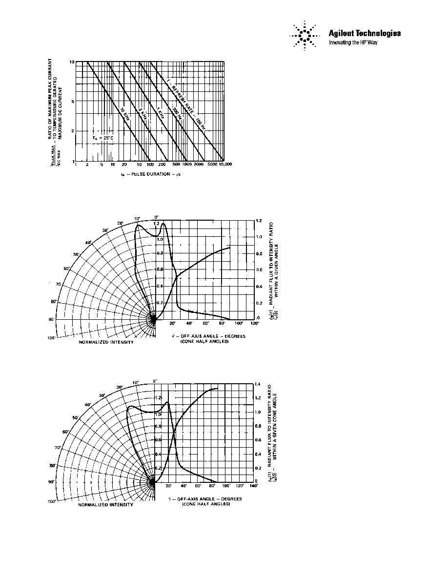
Figure 8. Far Field Radiation Pattern, HEMT-3301.
Figure 7. Maximum Tolerable Peak Current vs. Peak Duration (I
PEAK MAX
Determined from Temperature Derated I
DC MAX
).
Figure 9. Far Field Radiation Pattern, HEMT-1001.
www.semiconductor.agilent.com
Data subject to change.
Copyright © 1999 Agilent Technologies, Inc.
Obsoletes 5954-8473E
5964-3813E (11/99)