 | –≠–ª–µ–∫—Ç—Ä–æ–Ω–Ω—ã–π –∫–æ–º–ø–æ–Ω–µ–Ω—Ç: HFBR-0561 | –°–∫–∞—á–∞—Ç—å:  PDF PDF  ZIP ZIP |
Document Outline
- Features
- Applications
- Description
- ATM 2 km Backbone Links
- Transmitter Sections
- Receiver Sections
- Ordering Information
- Package
- Figure 1.
- Figure 2.
- Figure 3.
- Pin Descriptions:
- Application Information
- Transceiver Optical Power Budget versus Link Length
- Transceiver Signaling Operating Rate Range and BER Performance
- Figure 5.
- Figure 6.
- Solder and Wash Process Compatibility
- Transceiver Jitter Performance
- Recommended Handling Precautions
- Shipping Container
- Board Layout - Decoupling Circuit, Ground Planes and Termination Circuits
- Board Layout - Hole Pattern
- Board Layout - Art Work
- Regulatory Compliance
- Electrostatic Discharge (ESD)
- Electromagnetic Interference (EMI)
- Immunity
- Figure 10.
- Transceiver Reliability and Performance Qualification Data
- Applications Support Materials
- Absolute Maximum Ratings
- Recommended Operating Conditions
- Transmitter Electrical Characteristics
- Receiver Electrical Characteristics
- Transmitter Optical Characteristics
- Receiver Optical and Electrical Characteristics
- Notes:
Agilent HFBR-5905/5905A
ATM Multimode Fiber Transceivers
in 2 x 5 Package Style
Data Sheet
Description
The HFBR-5900 family of trans-
ceivers from Agilent provide the
system designer with products
to implement a range of
solutions for multimode fiber
SONET OC-3 (SDH STM-1)
physical layers for ATM and
other services.
These transceivers are all
supplied in the new industry
standard 2 x 5 DIP style with a
MT-RJ fiber connector interface.
ATM 2 km Backbone Links
The HFBR-5905 is a 1300 nm
product with optical
performance compliant with the
SONET STS-3c (OC-3) Physical
Layer Interface Specification.
This physical layer is defined in
the ATM Forum User-Network
Interface (UNI) Specification
Version 3.0. This document
references the ANSI T1E1.2
specification for the details of
the interface for 2 km multimode
fiber backbone links.
The ATM 100 Mb/s-125 MBd
Physical Layer interface is best
implemented with the HFBR-
5903 family of FDDI Transceiv-
ers which are specified for use
in this 4B/5B encoded physical
layer per the FDDI PMD
standard.
Transmitter Sections
The transmitter section of the
HFBR-5905 utilizes a 1300 nm
InGaAsP LED. This LED is
packaged in the optical
Features
∑ Multisourced 2 x 5 package style
with MT-RJ receptacle
∑ Single +3.3 V power supply
∑ Wave solder and aqueous wash
process compatibility
∑ Manufactured in an ISO 9002
certified facility
∑ Full compliance with ATM Forum
UNI SONET OC-3 multimode fiber
physical layer specification
Applications
∑ Multimode fiber ATM backbone
links
∑ Multimode fiber ATM wiring
closet to desktop links
Ordering Information
The HFBR-5905 1300 nm
product is available for
production orders through the
Agilent Component Field Sales
Offices and Authorized
Distributors world wide.
HFBR-5905
= 0∞C to +70∞C
HFBR-5905A = -40∞C to +85∞C.
subassembly portion of the
transmitter section. It is driven
by a custom silicon IC which
converts differential PECL logic
signals, ECL referenced (shifted)
to a +3.3 V supply, into an
analog LED drive current.
Receiver Sections
The receiver section of the
HFBR-5905 utilizes an InGaAs
PIN photodiode coupled to a
custom silicon transimpedance
preamplifier IC. It is packaged in
the optical subassembly portion
of the receiver.
This PIN/preamplifier combina-
tion is coupled to a custom
quantizer IC which provides the
final pulse shaping for the logic
output and the Signal Detect
function. The Data output is
differential. The Signal Detect
output is single-ended. Both
Data and Signal Detect outputs
are PECL compatible, ECL
referenced (shifted) to a 3.3 V
power supply. The receiver
outputs, Data Out and Data Out
Bar, are squelched at Signal
Detect Deassert. That is, when
the light input power decreases
to a typical -38 dBm or less, the
Signal Detect Deasserts, i.e. the
Signal Detect output goes to a
PECL low state. This forces the
receiver outputs, Data Out and
Data Out Bar to go to steady
PECL levels High and Low
respectively.
2
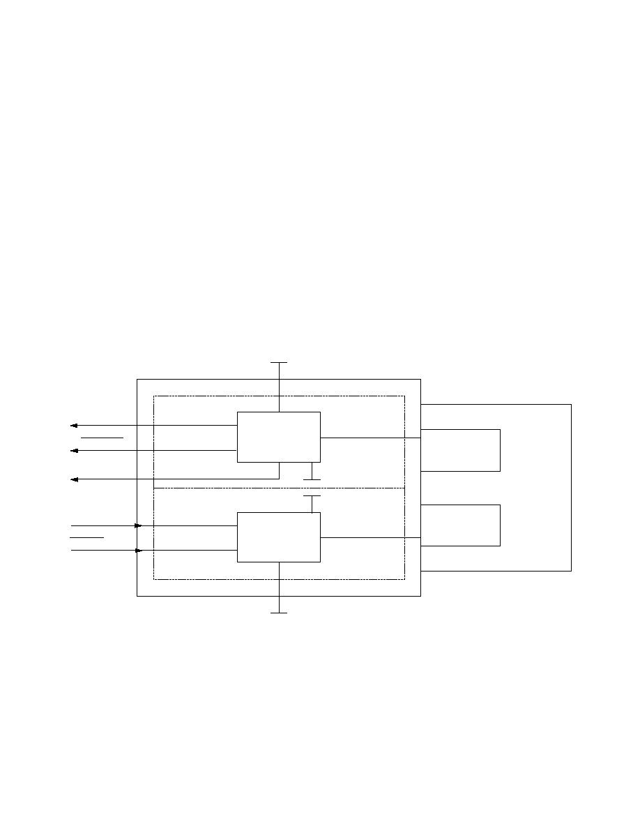
Package
The overall package concept for
the Agilent transceiver consists
of three basic elements; the two
optical subassemblies, an
electrical subassembly, and the
housing as illustrated in the
block diagram in Figure 1.
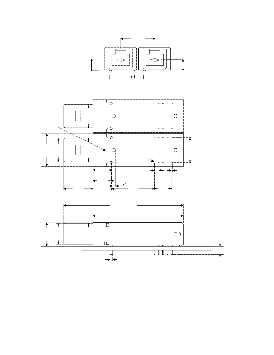
The package outline drawing
and pin out are shown in
Figures 2 and 3. The details of
this package outline and pin out
are compliant with the multi-
source definition of the 2 x 5
DIP. The low profile of the
Agilent transceiver design
complies with the maximum
height allowed for the MT-RJ
connector over the entire length
of the package.
The optical subassemblies utilize
a high-volume assembly process
together with low-cost lens
elements which result in a cost-
effective building block.
The electrical subassembly con-
sists of a high volume multilayer
printed circuit board on which
the IC and various surface-
mounted passive circuit
elements are attached.
The receiver section includes an
internal shield for the electrical
and optical subassemblies to
ensure high immunity to
external EMI fields.
The outer housing including the
MT-RJ ports is molded of filled
nonconductive plastic to provide
mechanical strength and
electrical isolation. The solder
posts of the Agilent design are
isolated from the internal circuit
of the transceiver.
The transceiver is attached to a
printed circuit board with the
ten signal pins and the two
solder posts which exit the
bottom of the housing. The two
solder posts provide the primary
mechanical strength to
withstand the loads imposed on
the transceiver by mating with
the MT-RJ connectored fiber
cables.
Figure 1. Block Diagram.
DATA OUT
SIGNAL
DETECT
DATA IN
QUANTIZER IC
LED DRIVER IC
PIN PHOTODIODE
PRE-AMPLIFIER
SUBASSEMBLY
LED
OPTICAL
SUBASSEMBLY
DATA OUT
DATA IN
MT-RJ
RECEPTACLE
R
X
SUPPLY
T
X
SUPPLY
R
X
GROUND
T
X
GROUND
3
Figure 2. Package Outline Drawing
FRONT VIEW
13.97
(0.55)
MIN.
4.5 ±0.2
(0.177 ±0.008)
(PCB to OPTICS
CENTER LINE)
5.15
(0.20)
(PCB to OVERALL
RECEPTACLE CENTER
LINE)
DIMENSIONS IN MILLIMETERS (INCHES)
NOTES:
1. THIS PAGE DESCRIBES THE MAXIMUM PACKAGE OUTLINE, MOUNTING STUDS, PINS AND THEIR RELATIONSHIPS TO EACH OTHER.
2. TOLERANCED TO ACCOMMODATE ROUND OR RECTANGULAR LEADS.
3. ALL 12 PINS AND POSTS ARE TO BE TREATED AS A SINGLE PATTERN.
4. THE MT-RJ HAS A 750 µm FIBER SPACING.
5. THE MT-RJ ALIGNMENT PINS ARE IN THE MODULE.
6. FOR SM MODULES, THE FERRULE WILL BE PC POLISHED (NOT ANGLED).
7. SEE MT-RJ TRANSCEIVER PIN OUT DIAGRAM FOR DETAILS.
37.56 (1.479) MAX.
SIDE VIEW
49.56 (1.951) REF.
9.8
(0.386)
MAX.
9.3
(0.366)
MAX.
ÿ 1.07
(0.042)
3.3
(0.13)
ÿ 0.61
(0.024)
Pin 1
TOP VIEW
9.6
(0.378)
MAX.
13.59
(0.535)
MAX.
12
(0.472)
7.59
(0.299)
8.6
(0.339)
ÿ1.5
(0.059)
17.778
(0.7)
1.778
(0.07)
7.112
(0.28)
+0
-0.2
(+000)
(-008)
10.16
(0.4)
Case temperature
measurement point

4
Figure 3. Pin Out Diagram.
Pin Descriptions:
Pin 1 Receiver Signal Ground V
EE
RX:
Directly connect this pin to the
receiver ground plane.
Pin 2 Receiver Power Supply V
CC
RX:
Provide +3.3 V dc via the
recommended receiver power
supply filter circuit. Locate the
power supply filter circuit as
close as possible to the V
CC
RX
pin.
Pin 3 Signal Detect SD:
Normal optical input levels to
the receiver result in a logic "1"
output.
Low optical input levels to the
receiver result in a fault
condition indicated by a logic
"0" output.
This Signal Detect output can be
used to drive a PECL input on
an upstream circuit, such as
Signal Detect input or Loss of
Signal-bar.
Pin 4 Receiver Data Out Bar RD-:
No internal terminations are
provided. See recommended
circuit schematic.
Pin 5 Receiver Data Out RD+:
No internal terminations are
provided. See recommended
circuit schematic.
Pin 6 Transmitter Power Supply
V
CC
TX:
Provide +3.3 V dc via the
recommended transmitter power
supply filter circuit. Locate the
power supply filter circuit as
close as possible to the V
CC
TX
pin.
Pin 7 Transmitter Signal Ground
V
EE
TX:
Directly connect this pin to the
transmitter ground plane.
Pin 8 Transmitter Disable T
DIS
:
No internal connection. Optional
feature for laser based products
only. For laser based products
connect this pin to +3.3 V TTL
logic high "1" to disable module.
To enable module connect to
TTL logic low "0".
Pin 9 Transmitter Data In TD+:
No internal terminations are
provided. See recommended
circuit schematic.
Pin 10 Transmitter Data In Bar TD-:
No internal terminations are
provided. See recommended
circuit schematic.
Mounting Studs/Solder Posts
The mounting studs are
provided for transceiver
mechanical attachment to the
circuit board. It is
recommended that the holes in
the circuit board be connected to
chassis ground.
TRANSMITTER DATA IN BAR
TRANSMITTER DATA IN
TRANSMITTER DISABLE (LASER BASED PRODUCTS ONLY)
TRANSMITTER SIGNAL GROUND
TRANSMITTER POWER SUPPLY
RX TX
o
o
o
o
o
1
2
3
4
5
o
o
o
o
o
10
9
8
7
6
RECEIVER SIGNAL GROUND
RECEIVER POWER SUPPLY
SIGNAL DETECT
RECEIVER DATA OUT BAR
RECEIVER DATA OUT
Top
View
Mounting Studs/
Solder Posts

5
Application Information
The Applications Engineering
group is available to assist you
with the technical under-
standing and design trade-offs
associated with these trans-
ceivers. You can contact them
through your Agilent sales
representative.
The following information is
provided to answer some of the
most common questions about
the use of these parts.
Transceiver Optical Power Budget
versus Link Length
Optical Power Budget (OPB) is
the available optical power for a
fiber optic link to accommodate
fiber cable losses plus losses due
to in-line connectors, splices,
optical switches, and to provide
margin for link aging and
unplanned losses due to cable
plant reconfiguration or repair.
Figure 4 illustrates the predicted
OPB associated with the
transceiver specified in this data
sheet at the Beginning of Life
(BOL). These curves represent
the attenuation and chromatic
plus modal dispersion losses
associated with the 62.5/125 µm
and 50/125 µm fiber cables only.
The area under the curves
represents the remaining OPB at
any link length, which is
available for overcoming non-
fiber cable related losses.
Agilent LED technology has
produced 1300 nm LED devices
with lower aging characteristics
than normally associated with
these technologies in the
industry. The industry conven-
tion is 1.5 dB aging for 1300 nm
LEDs. The
1300 nm Agilent LEDs are
specified to experience less than
1 dB of aging over normal com-
mercial equipment mission life
periods. Contact your Agilent
sales representative for
additional details.
Figure 4 was generated for the
1300 nm transceivers with a
Agilent fiber optic link model
containing the current industry
conventions for fiber cable
specifications and the draft
ANSI T1E1.2. These optical
parameters are reflected in the
guaranteed performance of the
transceiver specifications in this
data sheet. This same model has
been used extensively in the
ANSI and IEEE committees,
including the ANSI T1E1.2
committee, to establish the
optical performance
requirements for various fiber
optic interface standards. The
cable parameters used come
from the ISO/IEC JTC1/SC
25/WG3 Generic Cabling for
Customer Premises per DIS
11801 document and the EIA/
TIA-568-A Commercial Building
Telecommunications Cabling
Standard per SP-2840.
Transceiver Signaling Operating
Rate Range and BER Performance
For purposes of definition, the
symbol (Baud) rate, also called
signaling rate, is the reciprocal
of the symbol time. Data rate
(bits/sec) is the symbol rate
divided by the encoding factor
used to encode the data
(symbols/bit).
When used in 155 Mb/s SONET
OC-3 applications the perform-
ance of the 1300 nm trans-
ceivers, HFBR-5905 is
guaranteed to the full conditions
listed in product specification
tables.
The transceivers may be used
for other applications at signal-
ing rates different than 155 Mb/s
with some variation in the link
optical power budget. Figure 5
gives an indication of the typical
performance of these products
at different rates.
These transceivers can also be
used for applications which
require different Bit Error Rate
(BER) performance. Figure 6
illustrates the typical trade-off
between link BER and the
receivers input optical power
level.
Figure 4. Typical Optical Power Budget at BOL
versus Fiber Optic Cable Length.
Figure 5. Transceiver Relative Optical Power
Budget at Constant BER vs. Signaling Rate.
OPTICAL POW
ER BUDGET (dB)
0
FIBER OPTIC CABLE LENGTH (km)
0.5
1.5
2.0
2.5
12
10
8
6
4
2
1.0
0.
3
HFBR-5905, 62.5/125 µm
HFBR-5905
50/125 µm
CONDITIONS:
1. PRBS 2
7
-1
2. DATA SAMPLED AT CENTER OF DATA SYMBOL.
3. BER = 10
-6
4. T
A
= +25 C
5. V
CC
= 3.3 V dc
6. INPUT OPTICAL RISE/FALL TIMES = 1.0/2.1 ns.
-1
-0.5
0
0.5
1
1.5
2
2.5
0
25
50
75
100
125
150
175
200
SIGNAL RATE (MBd)
TRANSCEIVER RELATIVE POWER BUDGET
AT CONSTANT BER (dB)