Document Outline
- List of Figures
- 1. Transmitter and Receiver Block Diagram.
- 2. Package Outline Drawing.
- 3. Pinout Drawing.
- 4. Optical Power Budget at BOL vs. Fiber Optic Cable Length
- 5. Transmitter/Receiver Relative Optical Power Budget at Constant BER vs. Signaling Rate
- 6. Bit Error Ratio vs. Relative Receiver Input Optical Power
- 7. Recommended Interface Circuitry and Power Supply Filter Circuits
- 8. Recommended Board Layout Hole Pattern
- 9. HFBR-1116T Transmitter Output Optical Spectral Width (FWHM) vs. Transmitter Output Optical Center Wavelength and Rise/ Fall T
- 10. HFBR-2116T Receiver Input Optical Power vs. Eye Sampling Time Position
- Features
- Applications
- Description
- Transmitter
- Receiver
- Package
- Application Information
- Transmitter and Receiver Optical Power Budget versus Link Length
- Transmitter and Receiver Signaling Rate Range and BER Performance
- Data Link Jitter Performance
- Recommended Handling Precautions
- Solder and Wash Process Compatibility
- Shipping Container
- Board LayoutÖInterface Circuit and Layout Guidelines
- Board LayoutÖHole Pattern
- Regulatory Compliance
- HFBR-1116T Transmitter Pin-Out Table
- HFBR-2116T Receiver Pin-Out Table
- SpecificationsÖAbsolute Maximum Ratings
- Recommended Operating Conditions
- HFBR-1116T Transmitter Electrical Characteristics
- HFBR-2116T Receiver Electrical Characteristics
- HFBR-1116T Transmitter Optical Characteristics
- HFBR-2116T Receiver Optical Characteristics
189
Fiber Optic Transmitter
and Receiver Data Links
for 155 MBd
Technical Data
HFBR-1116T Transmitter
HFBR-2116T Receiver
Description
The HFBR-1116/-2116 series of
data links are high-performance,
cost-efficient, transmitter and
receiver modules for serial
optical data communication
applications specified at 155 MBd
for ATM UNI applications.
These modules are designed for
50 or 62.5
µ
m core multimode
optical fiber and operate at a
nominal wavelength of 1300 nm.
They incorporate our high-
performance, reliable, long-
wavelength, optical devices and
proven circuit technology to give
long life and consistent
performance.
Transmitter
The transmitter utilizes a 1300 nm
surface-emitting InGaAsP LED,
packaged in an optical subassem-
bly. The LED is dc-coupled to a
custom IC which converts
differential-input, PECL logic
signals, ECL-referenced (shifted)
to a +5 V power supply, into an
analog LED drive current.
Receiver
The receiver utilizes an InGaAs
PIN photodiode coupled to a
custom silicon transimpedance
Features
∑ Full Compliance with the
Optical Performance
Requirements of the ATM
Forum UNI SONET OC-3
Multimode Physical Layer
Specification
∑ Other Versions Available for:
- FDDI
- Fibre Channel
∑ Compact 16-pin DIP Package
with Plastic ST* Connector
∑ Wave Solder and Aqueous
Wash Process Compatible
Package
∑ Manufactured in an ISO
9001 Certified Facility
Applications
∑ ATM Switches, Hubs, and
Network Interface Cards
∑ Multimode Fiber ATM
Wiring Closet-to-Desktop
Links
∑ Point-to-Point Data
Communications
∑ Replaces DLT/R1040-ST1
Model Transmitters and
Receivers
preamplifier IC. The PIN-
preamplifier combination is ac-
coupled to a custom quantizer IC
which provides the final pulse
shaping for the logic output and
the Signal Detect function. Both
the Data and Signal Detect
Outputs are differential. Also,
both Data and Signal Detect
Outputs are PECL compatible,
ECL-referenced (shifted) to a
+5 V power supply.
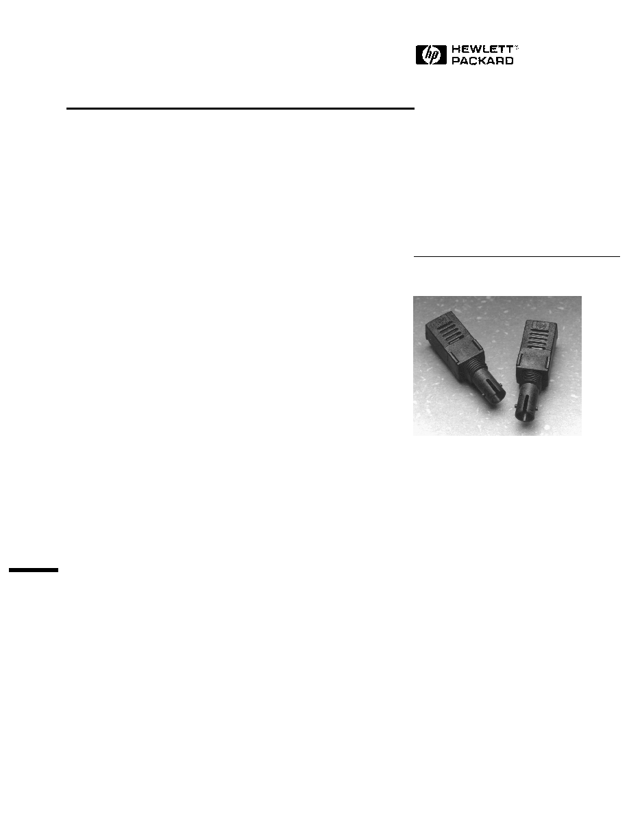
Package
The overall package concept for
the Data Links consists of the
following basic elements: two
optical subassemblies, two
electrical subassemblies, and the
outer housings as illustrated in
Figure 1.
*ST is a registered trademark of AT&T Lightguide Cable Connectors.
5965-3482E (8/96)

190
DATA IN
SIGNAL
DETECT OUT
DATA IN
RECEIVER
QUANTIZER
IC
DRIVER IC
TOP VIEW
PIN PHOTODIODE
OPTICAL
SUBASSEMBLIES
PREAMP IC
DIFFERENTIAL
DIFFERENTIAL
DIFFERENTIAL
VBB
TRANSMITTER
LED
ELECTRICAL
SUBASSEMBLIES
SIMPLEX STÆ
RECEPTACLE
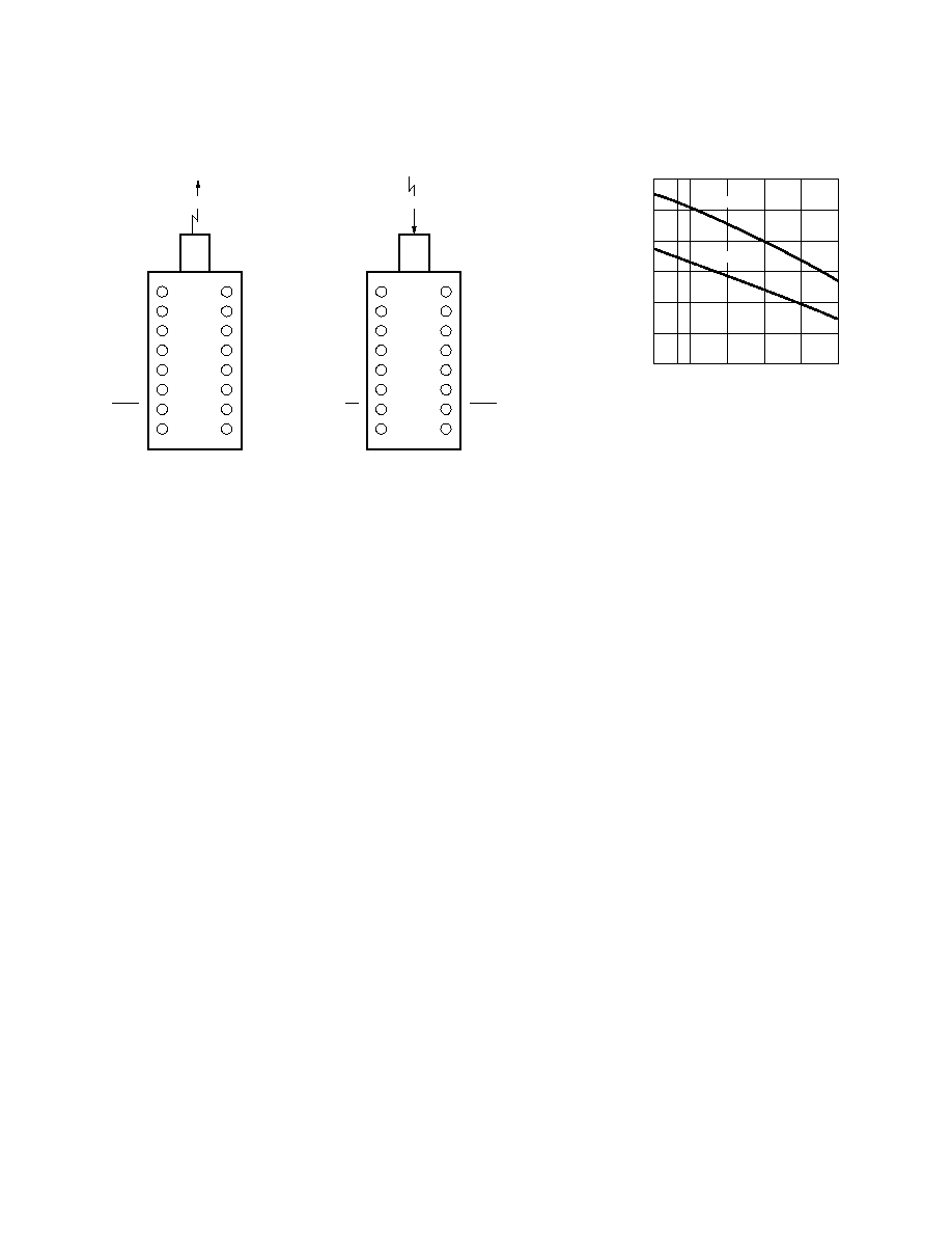
The package outline drawing and
pinout are shown in Figures 2
and 3. The details of this package
outline and pinout are compatible
with other data-link modules from
other vendors.
The optical subassemblies consist
of a transmitter subassembly in
which the LED resides and a
receiver subassembly housing the
PIN-preamplifier combination.
The electrical subassemblies con-
sist of a multi-layer printed circuit
board on which the IC chips and
various surface-mounted, passive
circuit elements are attached.
Figure 1. Transmitter and Receiver Block Diagram.
Figure 2. Package Outline Drawing.
41 MAX.
8.31
12.19
MAX.
THREADS
3/8 ≠ 32 UNEF-2A
HFBR-111X/211XT
DATE CODE (YYWW)
SINGAPORE
5.05
19.72
2.45
7.01
5.0
9.8 MAX.
3
0.9
PCB PINS
DIA. 0.46 mm
NOTE 2
8 x 7.62
17.78
(7 x 2.54)
12
HOUSING PINS 0.38 x 0.5 mm
NOTE 1
NOTES:
1. MATERIAL ALLOY 194 1/2H ≠ 0.38 THK
FINISH MATTE TIN PLATE 7.6 µm MIN.
2. MATERIAL PHOSPHOR BRONZE WITH
120 MICROINCHES TIN LEAD (90/10)
OVER 50 MICROINCHES NICKEL.
3. UNITS = mm
191
Each transmitter and receiver
package includes an internal shield
for the electrical subassembly to
ensure low EMI emissions and high
immunity to external EMI fields.
The outer housing, including the
ST* port, is molded of filled, non-
conductive plastic to provide
mechanical strength and electrical
isolation. For other port styles,
please contact your Hewlett-
Packard Sales Representative.
Each data-link module is attached
to a printed circuit board via the
16-pin DIP interface. Pins 8 and 9
provide mechanical strength for
these plastic-port devices and will
provide port-ground for forthcom-
ing metal-port modules.
Application Information
The Applications Engineering
group of the Optical Communi-
cation Division is available to assist
you with the technical understand-
ing and design tradeoffs associated
with these transmitter and receiver
modules. You can contact them
through your Hewlett-Packard
sales representative.
The following information is
provided to answer some of the
most common questions about the
use of these parts.
Transmitter and Receiver
Optical Power Budget
versus Link Length
The Optical Power Budget (OPB)
is the available optical power for a
fiber-optic link to accommodate
fiber cable losses plus losses due to
in-line connectors, splices, optical
switches, and to provide margin for
link aging and unplanned losses
due to cable plant reconfiguration
or repair.
Figure 4 illustrates the predicted
OPB associated with the trans-
mitter and receiver specified in this
data sheet at the Beginning of Life
(BOL). This curve represents the
attenuation and chromatic plus
modal dispersion losses associated
with 62.5/125
µ
m and 50/125
µ
m
fiber cables only. The area under
the curve represents the remaining
OPB at any link length, which is
available for overcoming non-fiber
cable related losses.
Figure 3. Pinout Drawing.
NC
8
9
NC
GND
7
10
NO PIN
VCC
6
11
GND
VCC
5
12
GND
GND
4
13
GND
DATA
3
14
GND
DATA
2
15
VBB
NC
1
16
NC
OPTICAL PORT
TRANSMITTER
NC
8
9
NC
NO PIN
7
10
GND
GND
6
11
VCC
GND
5
12
VCC
GND
4
13
VCC
SD
3
14
DATA
SD
2
15
DATA
NO PIN
1
16
NC
OPTICAL PORT
RECEIVER
Figure 4. Optical Power Budget at
BOL vs. Fiber Optic Cable Length.
OPTICAL POWER BUDGET (dB)
0
FIBER OPTIC CABLE LENGTH (km)
0
1.0
1.5
12
10
8
4
2.5
2
0.3
2.0
6
0.5
62.5/125 µm
50/125 µm
*ST is a registered trademark of AT&T Lightguide Cable Connectors.
192
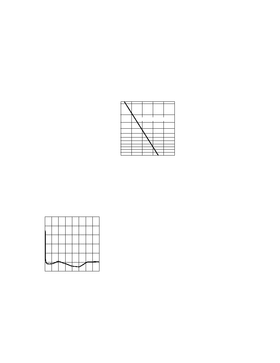
Transmitter and Receiver
Signaling Rate Range and
BER Performance
For purposes of definition, the
symbol rate (Baud), also called
signaling rate, is the reciprocal of
the symbol time. Data rate (bits/
sec) is the symbol rate divided by
the encoding factor used to encode
the data (symbols/bit).
When used in 115 Mbps SONET
OC-3 applications, the perform-
ance of Hewlett-Packard's
1300 nm data link modules, HFBR-
1116/-2116, is guaranteed to the
full conditions listed in the individ-
ual product specification tables.
The data link modules may be used
for other applications at signaling
rates different than the 155 Mbps
with some variation in the link
optical power budget. Figure 5
gives an indication of the typical
performance of these 1300 nm
products at different rates.
These data link modules can also
be used for applications which
require different bit-error-ratio
(BER) performance. Figure 6
illustrates the typical trade-off
between link BER and the receiver
input optical power level.
The jitter specifications stated in
the following transmitter and
receiver specification table are
derived from the values in Table
B1 of Annex B. They represent the
worst-case jitter contribution that
the transmitter and receiver are
allowed to make to the overall
system jitter without violating the
Annex B allocation example. In
practice, the typical jitter
contribution of the Hewlett-
Packard data link modules is well
below the maximum allowed
amounts.
Recommended Handling
Precautions
It is advised that normal static pre-
cautions be taken in the handling
and assembly of these data link
modules to prevent damage which
may be induced by electrostatic
discharge (ESD). The HFBR-1116/-
2116 series meets MIL-STD-883C
Method 3015.4 Class 2.
Care should be taken to avoid
shorting the receiver Data or
Signal Detect Outputs directly to
ground without proper current-
limiting impedance.
Solder and Wash Process
Compatibility
The transmitter and receiver are
delivered with protective process
caps covering the individual ST*
ports. These process caps protect
the optical subassemblies during
wave solder and aqueous wash
processing and act as dust covers
during shipping.
These data link modules are
compatible with either industry
standard wave- or hand-solder
processes.
Figure 5. Transmitter/Receiver
Relative Optical Power Budget at
Constant BER vs. Signaling Rate.
TRANSMITTER/RECEIVER RELATIVE OPTICAL
POWER BUDGET AT CONSTANT BER (dB)
0
200
0
SIGNAL RATE (MBd)
25
75
100 125
2.5
2.0
1.5
1.0
175
0.5
50
150
CONDITIONS:
1. PRBS 2
7
-1
2. DATA SAMPLED AT CENTER OF DATA SYMBOL.
3. BER = 10
-6
4. TA = 25∞ C
5. VCC = 5 Vdc
6. INPUT OPTICAL RISE/FALL TIMES = 1.0/2.1 ns.
0.5
Figure 6. Bit Error Ratio vs. Relative
Receiver Input Optical Power.
BIT ERROR RATIO
-6
4
1 x 10
-2
RELATIVE INPUT OPTICAL POWER ≠ dB
-4
2
-2
0
1 x 10
-4
1 x 10
-6
1 x 10
-8
1 x 10
-10
1 x 10
-11
CONDITIONS:
1. 155 MBd
2. PRBS 2
7
-1
3. T
A
= 25∞ C
4. V
CC
= 5 Vdc
5. INPUT OPTICAL RISE/FALL TIMES = 1.0/2.1 ns.
1 x 10
-12
1 x 10
-9
1 x 10
-7
1 x 10
-5
1 x 10
-3
CENTER OF SYMBOL
Data Link Jitter
Performance
The Hewlett-Packard 1300 nm data
link modules are designed to
operate per the system jitter
allocations stated in Table B1 of
Annex B of the ANSI T1E1.2
Revision 3 standard.
The 1300 nm transmitter will
tolerate the worst-case input
electrical jitter allowed in Annex B
without violating the worst-case
output jitter requirements.
The 1300 nm receiver will tolerate
the worst-case input optical jitter
allowed in Annex B without
violating the worst-case output
electrical jitter allowed.
193
NC 8
9 NC
7
10 GND
GND 6
11 V
CC
GND 5
12 V
CC
GND 4
13 GND
GND 3
14 D
V
BB
2
15 D
NC 1
16 NC
NO
PIN
Tx
A
C2
0.1
*
L2
1
R3
82
R4
130
R2
82
R1
130
C5
0.1
+5 Vdc
GND
DATA
DATA
TERMINATE D, D
AT Tx INPUTS
*
Shipping Container
The data link modules are
packaged in a shipping container
designed to protect it from
mechanical and ESD damage
during shipment or storage.
Board Layout≠Interface
Circuit and Layout
Guidelines
It is important to take care in the
layout of your circuit board to
achieve optimum performance
from these data link modules.
Figure 7 provides a good example
of a power supply filter circuit that
works well with these parts. Also,
suggested signal terminations for
the Data, Data-bar, Signal Detect
and Signal Detect-bar lines are
shown. Use of a multilayer,
ground-plane printed circuit board
will provide good high-frequency
circuit performance with a low
inductance ground return path. See
additional recommendations noted
in the interface schematic shown in
Figure 7.
Figure 7. Recommended Interface Circuitry and Power Supply Filter Circuits.
NOTES:
1. RESISTANCE IS IN OHMS. CAPACITANCE IS IN MICROFARADS. INDUCTANCE IS IN MICROHENRIES.
2. TERMINATE TRANSMITTER INPUT DATA AND DATA-BAR AT THE TRANSMITTER INPUT PINS. TERMINATE THE RECEIVER OUTPUT DATA, DATA-BAR, AND SIGNAL DETECT-
BAR AT THE FOLLOW-ON DEVICE INPUT PINS. FOR LOWER POWER DISSIPATION IN THE SIGNAL DETECT TERMINATION CIRCUITRY WITH SMALL COMPROMISE TO THE
SIGNAL QUALITY, EACH SIGNAL DETECT OUTPUT CAN BE LOADED WITH 510 OHMS TO GROUND INSTEAD OF THE TWO RESISTOR, SPLIT-LOAD PECL TERMINATION
SHOWN IN THIS SCHEMATIC.
3. MAKE DIFFERENTIAL SIGNAL PATHS SHORT AND OF SAME LENGTH WITH EQUAL TERMINATION IMPEDANCE.
4. SIGNAL TRACES SHOULD BE 50 OHMS MICROSTRIP OR STRIPLINE TRANSMISSION LINES. USE MULTILAYER, GROUND-PLANE PRINTED CIRCUIT BOARD FOR BEST HIGH-
FREQUENCY PERFORMANCE.
5. USE HIGH-FREQUENCY, MONOLITHIC CERAMIC BYPASS CAPACITORS AND LOW SERIES DC RESISTANCE INDUCTORS. RECOMMEND USE OF SURFACE-MOUNT COIL
INDUCTORS AND CAPACITORS. IN LOW NOISE POWER SUPPLY SYSTEMS, FERRITE BEAD INDUCTORS CAN BE SUBSTITUTED FOR COIL INDUCTORS. LOCATE POWER
SUPPLY FILTER COMPONENTS CLOSE TO THEIR RESPECTIVE POWER SUPPLY PINS. C7 IS AN OPTIONAL BYPASS CAPACITOR FOR IMPROVED, LOW-FREQUENCY NOISE
POWER SUPPLY FILTER PERFORMANCE.
6. DEVICE GROUND PINS SHOULD BE DIRECTLY AND INDIVIDUALLY CONNECTED TO GROUND.
7. CAUTION: DO NOT DIRECTLY CONNECT THE FIBER-OPTIC MODULE PECL OUTPUTS (DATA, DATA-BAR, SIGNAL DETECT, SIGNAL DETECT-BAR, V
BB
) TO GROUND WITHOUT
PROPER CURRENT LIMITING IMPEDANCE.
8. (*) OPTIONAL METAL ST OPTICAL PORT TRANSMITTER AND RECEIVER MODULES WILL HAVE PINS 8 AND 9 ELECTRICALLY CONNECTED TO THE METAL PORT ONLY AND
NOT CONNECTED TO THE INTERNAL SIGNAL GROUND.
NC 8
9 NC
GND 7
10
V
CC
6
11 GND
V
CC
5
12 GND
V
CC
4
13 GND
D 3
14 SD
D
2
15 SD
NC 1
16
Rx
A
*
L1
1
R12
130
DATA
DATA
TERMINATE D, D, SD, SD AT
INPUTS OF FOLLOW-ON DEVICES
*
NO
PIN
NO
PIN
C1
0.1
C7
10
(OPTIONAL)
C3
0.1
C4
10
R6
130
R8
130
R5
82
R7
82
R9
82
C6
0.1
SD
R11
82
SD
R10
130
TOP VIEWS