HFBR-5204
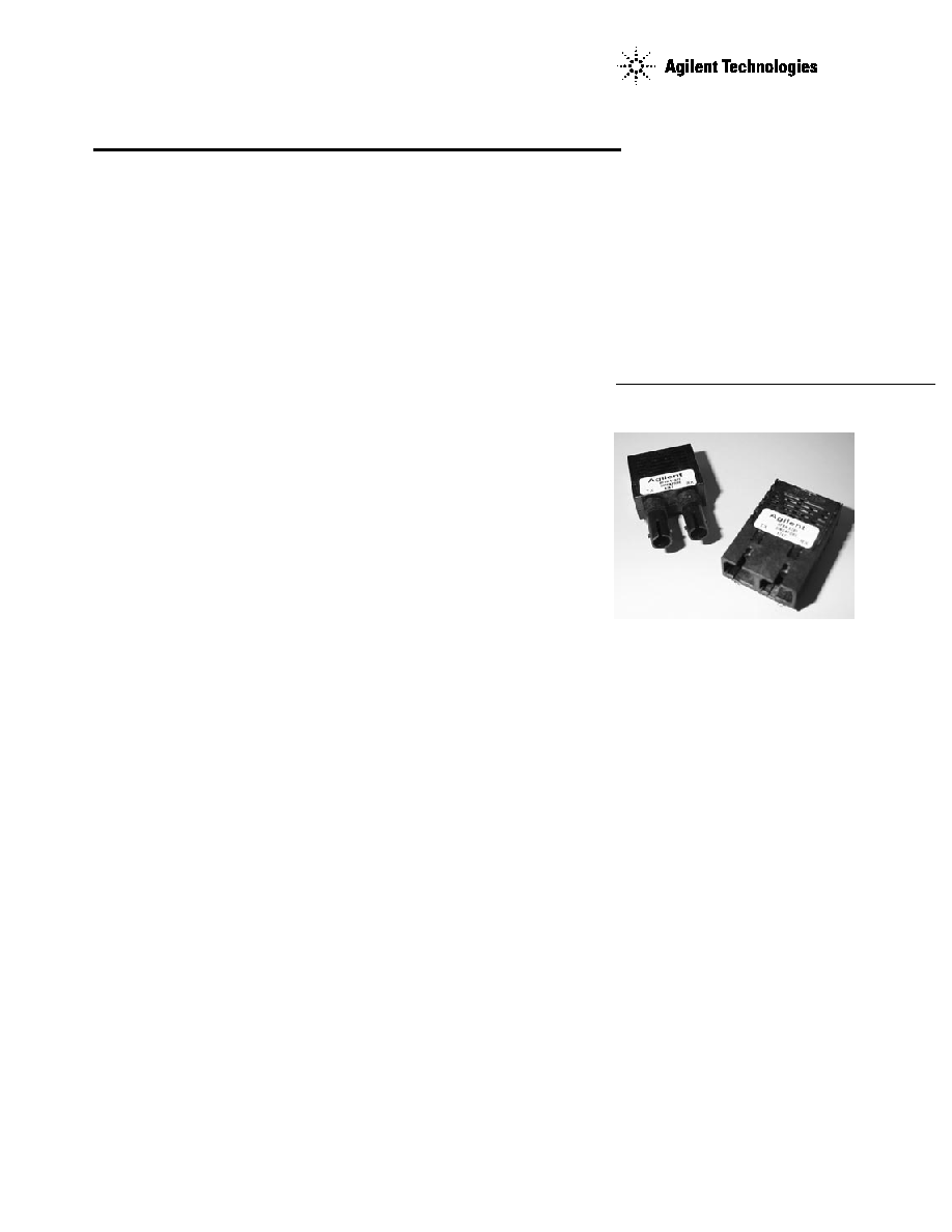
ATM Multimode Fiber
Transceivers for SONET
OC-3/SDH STM-1 in Low
Cost 1x9 Package Style
Data Sheet
Features
· Full Compliance with ATM
Forum UNI SONET OC-3
Multimode Fiber Physical
Layer Specification
· Multisourced 1 x 9 Package
Style with Choice of Duplex
SC or Duplex ST* Receptacle
· Wave Solder and Aqueous
Wash Process Compatibility
· Manufactured in an ISO 9002
Certified Facility
Applications
· Multimode Fiber ATM
Backbone Links
· Multimode Fiber ATM Wiring
Closet to Desktop Links
· ATM 155 Mbps/194 MBd
Encoded Links (available
upon special request)
Description
The HFBR-5200 family of trans-
ceivers from Agilent Technologies
provide the system designer with
products to implement a range of
solutions for multimode fiber
SONET OC-3 (SDH STM-1) physical
layers for ATM and other services.
These transceivers are all
supplied in the new industry
standard 1x9 SIP package style
with either a duplex SC or a
duplex ST* connector interface.
ATM 2000 m Backbone Links
The HFBR-5205/-5205T are
1300 nm products with optical
performance compliant with the
SONET STS-3c (OC-3) Physical
Layer Interface Specification. This
physical layer is defined in the
ATM Forum User-Network Inter-
face (UNI) Specification Version
3.0. This document references the
ANSI T1E1.2 specification for the
details of the interface for 2000
meter multimode fiber backbone
links.
Selected versions of these
transceivers may be used to
implement the ATM Forum UNI
Physical Layer Interface at the
155 Mbps/194 MBd rate.
The ATM 100 Mbps/125 MBd
Physical Layer interface is best
implemented with the HFBR-5100
family of FDDI Transceivers
which are specified for use in this
4B/5B encoded physical layer per
the FDDI PMD standard.
ATM 500 m Backbone and
Desktop Links
The HFBR-5204/-5204T are 1300
nm products which are similar to
the HFBR-5205/5205T except
that they are intended to provide
a lower cost SONET OC-3 link to
distances up to 500 meters in
62.5/125
µ
m multimode fiber
optic cables.
Transmitter Sections
The transmitter sections of the
HFBR-5204 and HFBR-5205
series utilize 1300 nm InGaAsP
LEDs. These LEDs are packaged
in the optical subassembly portion
of the transmitter section. They
are driven by a custom silicon IC
which converts differential PECL
logic signals, ECL referenced
(shifted) to a +5 Volt supply, into
an analog LED drive current.
HFBR-5204/-5204P/-5204T
1300 nm 500 m
HFBR-5205/-5205A/
-5205AT/-5205P/-5205T/
-5205PE
1300 nm 2 km
*ST is a registered trademark of AT&T Lightguide Cable Connectors.
2
Figures 2b and 2c show the
outline drawings for options that
include mezzanine height and
extended and flush shields
respectively.
The optical subassemblies utilize
a high volume assembly process
together with low cost lens
elements which result in a cost
effective building block.
The electrical subassembly con-
sists of a high volume multilayer
printed circuit board on which the
IC chips and various surface-
mounted passive circuit elements
are attached.
The package includes internal
shields for the electrical and
optical subassemblies to insure
low EMI emissions and high
immunity to external EMI fields.
The outer housing including the
duplex SC connector or the
duplex ST ports is molded of filled
non-conductive plastic to provide
mechanical strength and electrical
isolation. The solder posts of the
Agilent design are isolated from
the circuit design of the
transceiver and do not require
connection to a ground plane on
the circuit board.
The transceiver is attached to a
printed circuit board with the nine
signal pins and the two solder
posts which exit the bottom of the
housing. The two solder posts
provide the primary mechanical
strength to withstand the loads
imposed on the transceiver by
mating with the duplex or simplex
SC or ST connectored fiber
cables.
Note: The "T" in the product
numbers indicates a transceiver
with a duplex ST connector
receptacle. Product numbers
without a "T" indicate transceivers
with a duplex SC connector
receptacle.
Application Information
The Applications Engineering
group in the Agilent Optical
Communication Division is
available to assist you with the
technical understanding and
design trade-offs associated with
these transceivers. You can con-
tact them through your Agilent
sales representative.
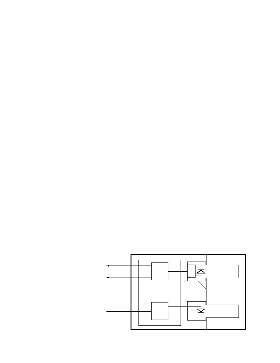
Figure 1. SC Block Diagram.
DATA OUT
SIGNAL
DETECT OUT
DATA IN
ELECTRICAL SUBASSEMBLY
QUANTIZER IC
DRIVER IC
TOP VIEW
PIN PHOTODIODE
DUPLEX SC
RECEPTACLE
OPTICAL
SUBASSEMBLIES
LED
PREAMP IC
DIFFERENTIAL
SINGLE-ENDED
DIFFERENTIAL
Receiver Sections
The receiver sections of the
HFBR-5204 and HFBR-5205
series utilize InGaAs PIN photo-
diodes coupled to a custom
silicon transimpedance preampli-
fier IC. These are packaged in the
optical subassembly portion of
the receiver.
These PIN/preamplifier combina-
tions are coupled to a custom
quantizer IC which provides the
final pulse shaping for the logic
output and the Signal Detect
function. The data output is
differential. The signal detect
output is single-ended. Both data
and signal detect outputs are
PECL compatible, ECL referenced
(shifted) to a +5 volt power
supply.
Package
The overall package concept for
the Agilent transceivers consists
of three basic elements; the two
optical subassemblies, an
electrical subassembly, and the
housing as illustrated in the block
diagrams in Figure 1 and
Figure 1a.
The package outline drawing and
pin out are shown in Figures 2,
2a, and 3. The details of this
package outline and pin out are
compliant with the multisource
definition of the 1x9 SIP. The low
profile of the Agilent transceiver
design complies with the
maximum height allowed for the
duplex SC connector over the
entire length of the package.
3
DATA OUT
SIGNAL
DETECT OUT
DATA IN
ELECTRICAL SUBASSEMBLY
QUANTIZER IC
DRIVER IC
TOP VIEW
PIN PHOTODIODE
DUPLEX ST
RECEPTACLE
OPTICAL
SUBASSEMBLIES
LED
PREAMP IC
DIFFERENTIAL
SINGLE-ENDED
DIFFERENTIAL
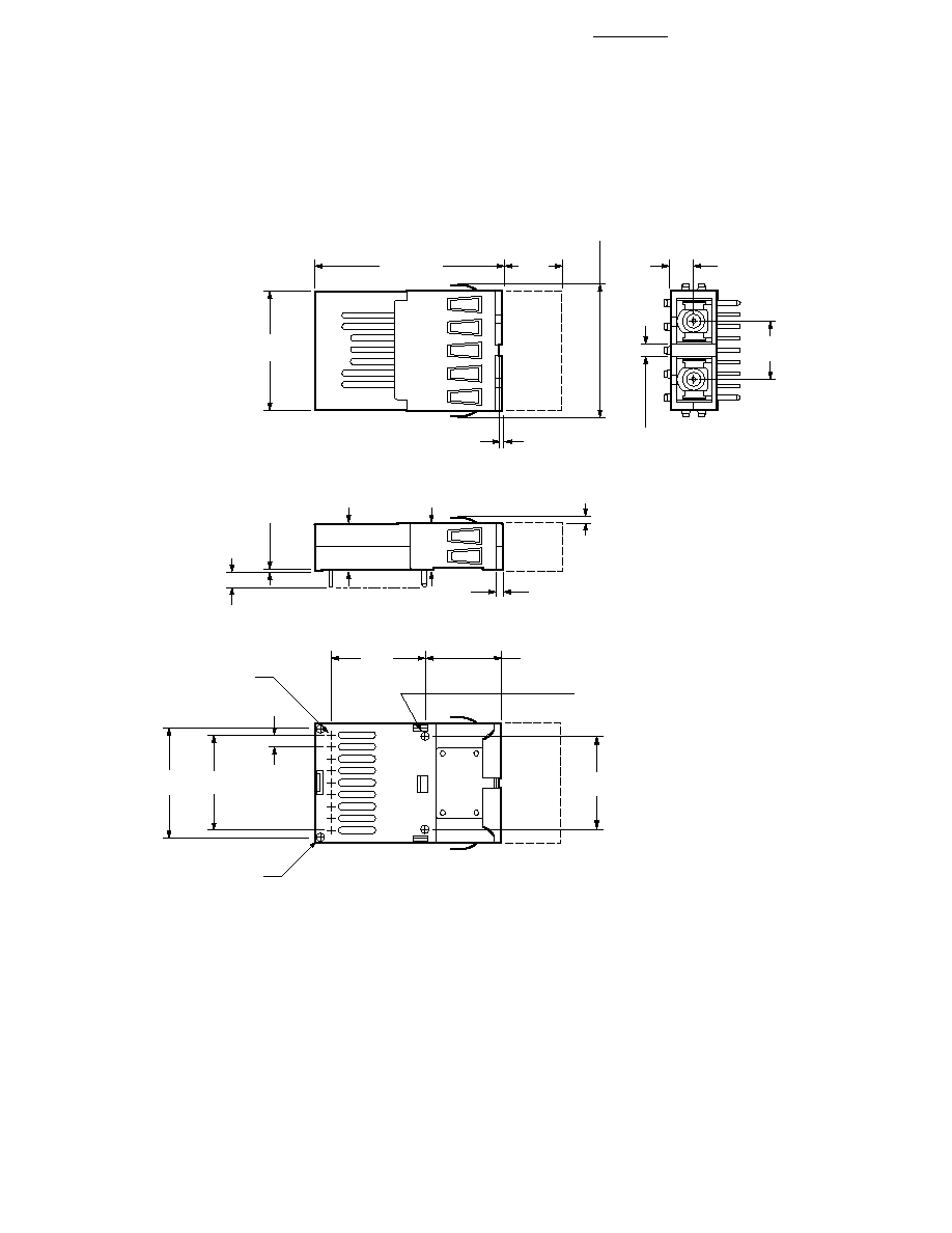
Figure 2. SC Package Outline Drawing with Standard Height.
Figure 1a. ST Block Diagram.
39.12
(1.540)
MAX.
AREA
RESERVED
FOR
PROCESS
PLUG
12.70
(0.500)
25.40
(1.000)
MAX.
12.70
(0.500)
10.35
(0.407)
MAX.
+ 0.25
- 0.05
+ 0.010
- 0.002
3.30 ± 0.38
(0.130 ± 0.015)
HFBR-5XXX
DATE CODE (YYWW)
SINGAPORE
2.92
(0.115)
18.52
(0.729)
4.14
(0.163)
20.32
(0.800)
[8x(2.54/.100)]
23.55
(0.927)
16.70
(0.657)
17.32
(0.682)
20.32
(0.800)
23.32
(0.918)
0.46
(0.018)
NOTE 1
(9x)
ø
NOTE 1
0.87
(0.034)
23.24
(0.915)
15.88
(0.625)
NOTE 1: THE SOLDER POSTS AND ELECTRICAL PINS ARE PHOSPHOR BRONZE WITH TIN LEAD OVER NICKEL PLATING.
DIMENSIONS ARE IN MILLIMETERS (INCHES).
1.27
(0.050
+ 0.08
- 0.05
+ 0.003
- 0.002
0.75
(0.030
)
)
A
6.35
(0.250)
5.93 ± 0.1
(0.233 ± 0.004)
4
Figure 2a. ST Package Outline Drawing with Standard Height.
25.4
(1.000)
MAX.
24.8
(0.976)
42
(1.654)
MAX.
5.99
(0.236)
12.7
(0.500)
12.0
(0.471)
MAX.
0.5
(0.020)
3.3 ± 0.38
(0.130) (± 0.015)
+ 0.08
- 0.05
+ 0.003
- 0.002
20.32 ± 0.38
(± 0.015)
HFBR-5103T
DATE CODE (YYWW)
SINGAPORE
3.2
(0.126)
2.6
(0.102)
22.86
(0.900)
20.32
(0.800)
[(8x (2.54/0.100)]
17.4
(0.685)
21.4
(0.843)
20.32
(0.800)
3.6
(0.142)
1.3
(0.051)
23.38
(0.921)
18.62
(0.733)
NOTE 1: PHOSPHOR BRONZE IS THE BASE MATERIAL FOR THE POSTS & PINS
WITH TIN LEAD OVER NICKEL PLATING.
DIMENSIONS IN MILLIMETERS (INCHES).
(
(
0.46
(0.018)
NOTE 1
+ 0.25
- 0.05
+ 0.010
- 0.002
(
(
1.27
0.050
5
Figure 2b. Package Outline Drawing with Mezzanine Height and Extended Shield.
39.6
(1.56)
MAX.
AREA
RESERVED
FOR
PROCESS
PLUG
12.70
(0.50)
25.4
(1.00)
MAX.
12.7
(0.50)
20.32
(0.800)
20.32
(0.800)
DIMENSIONS ARE IN MILLIMETERS (INCHES).
ALL DIMENSIONS ARE ± 0.025 mm UNLESS OTHERWISE SPECIFIED.
+0.1
-0.05
0.25
+0.004
-0.002
(
0.010
3.3 ± 0.38
(0.130 ± 0.015)
)
20.32
(0.80)
0.51
(0.02)
SLOT DEPTH
SLOT WIDTH
4.7
(0.185)
23.8
(0.937)
+0.25
-0.05
0.46
+0.010
-0.002
(
0.018
)
9X
1.3
(0.051)
2X
15.8 ± 0.15
(0.622 ± 0.006)
+0.25
-0.05
1.27
+0.010
-0.002
(
0.050
)
2X
2.0 ± 0.1
(0.079 ± 0.004)
29.6
(1.16)
8X 2.54
(0.100)
10.2
(0.40)
1.3
(0.05)
MAX.
2.09
(0.08)
UNCOMPRESSED
UNCOMPRESSED
9.8
(0.386)
MAX.
A