 | –≠–ª–µ–∫—Ç—Ä–æ–Ω–Ω—ã–π –∫–æ–º–ø–æ–Ω–µ–Ω—Ç: HFBR-5320 | –°–∫–∞—á–∞—Ç—å:  PDF PDF  ZIP ZIP |
200 MBd Low-Cost SBCON
Multimode Fiber Transceiver
Technical Data
Features
∑ Compliant with IBM
Enterprise Systems
Connection (ESCON)
Architecture
∑ Compliant to SBCON Draft
Specification (dpANS
X3.xxx-199x rev 2.2)
∑ Low Radiated Emissions and
High Immunity to Conducted
Noise
∑ Multi-Sourced 4 x 7 Package
Style with ESCON
Duplex
Connector Interface
∑ Wave Solder and Aqueous
Wash Process Compatible
∑ Manufactured in an ISO 9001
Certified Facility
∑ 1300 nm LED-Based
Transceiver
Applications
∑ Interconnection with IBM
Compatible Processors,
Directors, and Channel
Attachment Units
≠ Disk and Tape Drives
≠ Communication
≠
Controllers
∑ Data Communication
Equipment
≠ Local Area Networks
≠ Point-to-Point
≠
Communication
Note:
IBM, Enterprise System Connection
Architecture, ESCON, are registered
trademarks of International Business
Machines Corporation.
Description
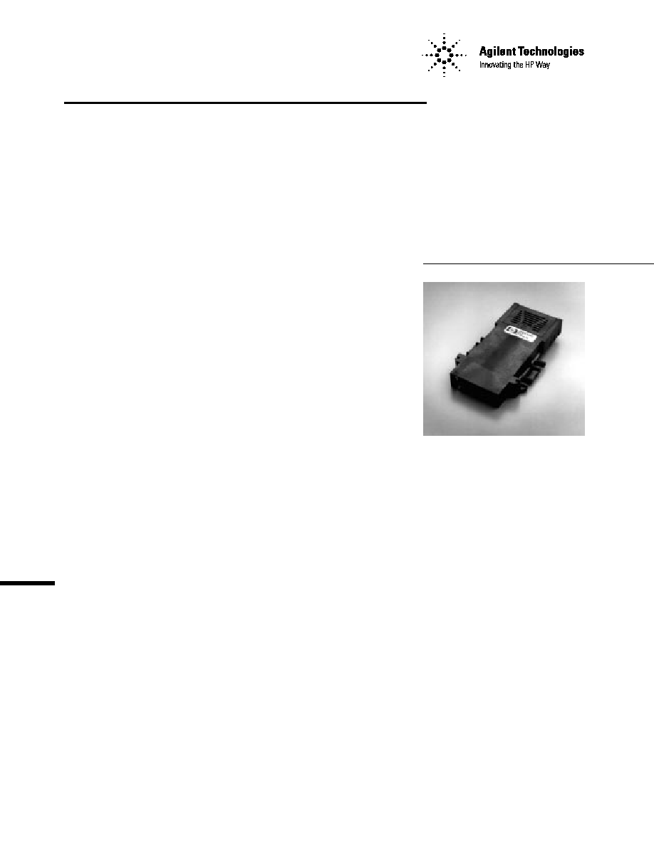
The HFBR-5320 SBCON
transceiver from Agilent provides
system designers with a product
to implement a range of solutions
compliant with the IBM
Enterprise System Connection
(ESCON)
architecture.
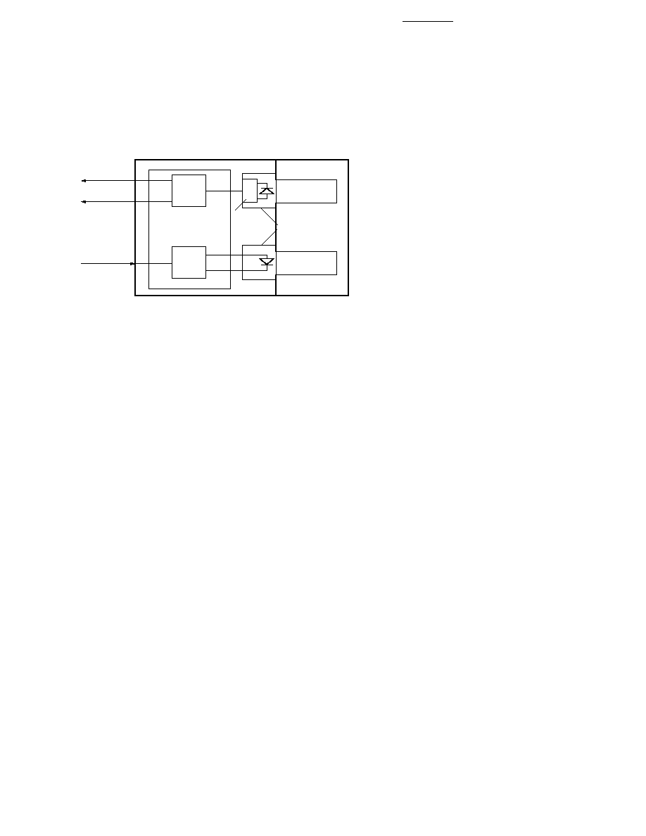
Transmitter Section
The transmitter section of the
HFBR-5320 utilizes 1300 nm
Surface Emitting InGaAsP LED.
The LED is packaged in an
optical sub-assembly within the
transmitter section. The LED is
driven by a custom silicon IC
which converts differential PECL
logic signals [ECL referenced
(shifted) to a +5 Volt supply]
into an analog LED drive current.
Receiver Section
The receiver section of the
HFBR-5320 utilizes an InGaAs
PIN photodiode coupled to a
custom silicon transimpedance
preamplifier IC. This PIN/
preamplifier combination is
coupled to a custom quantizer IC
which provides the final pulse
shaping for the logic Data Output
and Status Flag function. The
Data and Status Flag Outputs are
differential PECL compatible
[ECL referenced (shifted) to a +5
Volt power supply] logic outputs.
Package
The overall package concept for
the Agilent transceiver consists of
the following basic elements: two
optical sub-assemblies, an
electrical sub-assembly and the
housing with an integral duplex
SBCON connector receptacle.
This illustrated in Figure 1.
The package outline and pin-out
are shown in Figures 2 and 3.
The package includes internal
shields for the electrical and
optical sub-assemblies to ensure
low EMI emissions and high
immunity to EMI fields.
HFBR-5320
2
The optical sub-assemblies utilize
a high-volume assembly process
together with low-cost lens
technical understanding
associated with this transceiver.
You can contact them through
Solder and Wash Process
Compatibility
The transceiver is delivered with
a protective process plug inserted
into the duplex SBCON connector
receptacle. This process plug
protects the optical sub-
assemblies during wave solder
and aqueous wash processing and
acts as a dust cover during
shipping. These transceivers are
compatible with either industry
standard wave or hand soldering
processes. The process plug part
number is HFBR-5002.
Shipping Container
The transceiver is packaged in a
shipping container designed to
protect it from mechanical and
ESD damage during shipment or
storage.
Board Layout -
Decoupling Circuit and
Ground Planes
It is important to take care in the
layout of your circuit board to
achieve optimum performance
from the transceiver. Figure 3
provides a good example of a
schematic for a power supply
decoupling circuit that works well
with this part. It is further
recommended that a contiguous
ground plane be provided in the
circuit board directly under the
transceiver to provide a low
inductive ground for signal return
current. This recommendation is
in keeping with good high-
frequency board layout practices.
Note:
Ultem is a registered trademark of
General Electric Corporation.
elements which result in a cost-
effective building block.
The electrical subassembly
consists of a high-volume multi-
layer printed circuit board on
which the IC circuits and various
surface-mount passive circuit
elements are attached.
The outer housing, including the
SBCON-compliant duplex
connector receptacle, is molded
of filled, non-conductive UL 94V-
0 flame retardant Ultem
plastic
(U.L. File E121562) to provide
mechanical strength and
electrical isolation.
The transceiver is attached to a
printed circuit board with 28
signal pins (4 rows of 7 pins) and
with the four slots on the flanges
which are located on the package
sides. These four slots on the
flanges provide the primary
mechanical strength to withstand
the loads imposed by the duplex
connectored fiber cables.
Applications Information
The Applications Engineering
group in the Agilent Optical
Communications Division is
available to assist you with the
your local Agilent sales
representative.
Agilent LED technology has
produced 1300 nm LED devices
with lower aging characteristics
than normally associated with
these technologies in the
industry. The industry convention
is 1.5 dB aging for 1300 nm
LEDs. The Agilent LED will
normally experience less than
half this amount of aging over
normal, commercial equipment
mission-life periods. Contact your
local Agilent sales representatives
for additional details.
Recommended Handling
Precautions
It is advised that normal, anti-
static precautions be taken in the
handling and assembly of these
transceivers to prevent damage
which may be induced by
electrostatic discharge (ESD).
The HFBR-5320 transceiver
meets Mil-Std-883C Method
3015.4 Class 2.
Care should be used to avoid
shorting the receiver Data or
Status Flag Outputs directly to
ground without proper current
limiting impedance.
Figure 1. Block Diagram.
DATA OUT
SIGNAL
DETECT OUT
DATA IN
ELECTRICAL SUBASSEMBLY
QUANTIZER IC
DRIVER IC
TOP VIEW
PIN
PHOTODIODE
DUPLEX
RECEPTACLE
OPTICAL
SUBASSEMBLIES
LED
PREAMP
IC
DIFFERENTIAL
DIFFERENTIAL
DIFFERENTIAL

3
Regulatory Compliance
This transceiver product is
intended to enable commercial
system designers to develop
equipment that complies with the
various international regulations
governing certification of
Information Technology
Equipment. See the Regulatory
Compliance Table for details.
Additional information is
benches, and floor mats in ESD
controlled areas.
The second case to consider is
static discharges to the exterior
of the equipment chassis
containing the transceiver parts.
To the extent that the SBCON-
compatible duplex connector
receptacle is exposed to the
outside of the equipment chassis,
available from your local Agilent
sales representative.
Electrostatic Discharge
(ESD)
There are two design cases in
which immunity to ESD damage
is important.
The first case is during handling
of the transceiver prior to
mounting it on the circuit board.
It is important to use normal ESD
handling precautions for ESD
sensitive devices. These
precautions include using
grounded wrist straps, work
it may be subject to whatever
ESD system level test criteria that
the equipment is intended to
meet.
Electromagnetic
Interference (EMI)
Most equipment designs utilizing
this high-speed transceiver from
Agilent will be required to meet
the requirements of FCC in the
United States, CENELEC
EN55022 (CISPR 22) in Europe
and VCCI in Japan.
This device is suitable for a
variety of applications utilizing
the IBM
ESCON
/ SBCON
architecture.
Immunity
Equipment utilizing this
transceiver will be subject to radio-
frequency electromagnetic fields in
some environments. This
transceiver has a high immunity to
such fields.
Ordering Information
The HFBR-5320 1300 nm SBCON-
compatible transceiver is available
for production orders through the
Agilent Component Field Sales
Offices and Authorized Distributors
worldwide.
All HFBR-5320 LED transmitters are classified as IEC-825-1 Accessible Emission Limit (AEL) Class 1 based upon the current
proposed draft scheduled to go into effect on January 1, 1997. AEL Class 1 LED devices are considered eye safe.
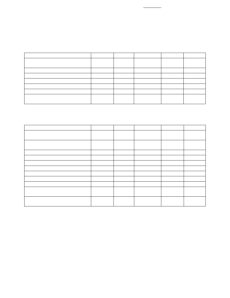
Regulatory Compliance Table
Feature
Test Method
Performance
Electrostatic Discharge (ESD) to
MIL-STD-883C
Meets Class 2 (2000 to 3999 Volts) Withstands up
the Electrical Pins
Method 3015.4
to 2200 V applied between electrical pins.
Electrostatic Discharge (ESD) to
Variation of IEC 801-2
Typically withstand at least 25kV without damage
the Duplex SBCON Receptacle
when the Duplex SBCON Connector Receptacle is
contacted by a Human Body Model probe.
Electromagnetic Interference
FCC Class B
Typically provide a 20 dB margin to the noted
(EMI)
CENELEC EN55022
standard limits when tested at a certified test range
Class B (CISPR 22B)
with the transceiver mounted to a circuit card
VCCI Class 2
without a chassis enclosure.
Immunity
Variation of IEC 801-3
Typically show no measurable effect from a 10V/m
field swept from 10 to 450 MHz applied to the
transceiver when mounted to a circuit card without
a chassis enclosure.

4
Absolute Maximum Ratings
Parameter
Symbol
Min.
Typ.
Max.
Unit
Reference
Storage Temperature
T
S
≠ 40
100
∞
C
Lead Soldering Temperature
T
SOLD
260
∞
C
Lead Soldering Time
t
SOLD
10
sec.
Supply Voltage
V
CC
≠ 0.5
7.0
V
Data Input Voltage
V
I
≠ 0.5
V
CC
V
Differential Input Voltage
V
D
1.4
V
Note 1
Output Current
I
O
50
mA
Recommended Operating Conditions
Parameter
Symbol
Min.
Typ.
Max.
Unit
Reference
Ambient Operating Temperature
T
A
0
70
∞
C
Supply Voltage
V
CC
4.75
5.25
V
Data Input Voltage - Low
V
IL
- V
CC
≠1.890
≠1.475
V
Data Input Voltage - High
V
IH
- V
CC
≠1.165
≠0.810
V
Data and Status Flag Output Load
R
L
50
Note 2
Transmitter Electrical Characteristics
(T
A
= 0
∞
C to 70
∞
C, V
CC
= 4.75 V to 5.25 V)
Parameter
Symbol
Min.
Typ.
Max.
Unit
Reference
Supply Current
I
CC
145
185
mA
Note 3
Power Dissipation
P
DISS
0.76
0.97
W
Data Input Current - Low
I
IL
≠ 350
µ
A
Data Input Current - High
I
IH
350
µ
A
Threshold Voltage
V
BB
- V
CC
≠ 1.42
≠ 1.3
≠ 1.24
V
Note 21
Receiver Electrical Characteristics
(T
A
= 0
∞
C to 70
∞
C, V
CC
= 4.75 V to 5.25 V)
Parameter
Symbol
Min.
Typ.
Max.
Unit
Reference
Supply Current
I
CC
100
125
mA
Note 4
Power Dissipation
P
DISS
0.3
0.5
W
Note 5
Data Output Voltage - Low
V
OL
- V
CC
≠1.890
≠1.620
V
Note 6
Data Output Voltage - High
V
OH
- V
CC
≠1.060
≠0.810
V
Note 6
Data Output Rise Time
t
r
0.35
1.3
ns
Note 7
Data Output Fall Time
t
f
0.35
1.3
ns
Note 7
Status Flag Output Voltage - Low
V
OL
- V
CC
≠1.890
≠1.620
V
Note 6
Status Flag Output Voltage - High
V
OH
- V
CC
≠1.060
≠0.810
V
Note 6
Status Flag Output Rise Time
t
r
0.35
2.2
ns
Note 7
Status Flag Output Fall Time
t
f
0.35
2.2
ns
Note 7
5
Transmitter Optical Characteristics
(T
A
= 0
∞
C to 70
∞
C, V
CC
= 4.75 V to 5.25 V)
Parameter
Symbol
Min.
Max.
Unit
Reference
Output Optical Power
P
O BOL
≠ 20.5
≠ 15.0
dBm
Note 9
62.5 / 125
µ
m, NA = 0.275 Fiber
P
O EOL
≠ 21.5
avg.
Optical Extinction Ratio
8
dB
Note 22
Center Wavelength
C
1280
1380
nm
Spectral Width - FWHM
175
nm
Note 11
Optical Rise Time
T
r
1.7
ns
Note 10, 12
Optical Fall Time
t
f
1.7
ns
Note 10, 12
Output Optical Systematic
t
SJ
0.8
ns
Note 13
Jitter
p-p
Receiver Optical and Electrical Characteristics
(T
A
= 0
∞
C to 70
∞
C, V
CC
= 4.75 V to 5.25 V)
Parameter
Symbol
Min.
Max.
Unit
Reference
Input Optical Power
P
IN
Min.
P
IN
Min. (C)
dBm avg.
Note 14
Minimum at Window Edge
(W)
+ 1.0 dB
Input Optical Power
P
IN
Min.
≠29.0
dBm avg.
Note 15
Minimum at Eye Center
(C)
Input Optical Power Maximum
P
IN
Max.
≠ 14.0
dBm avg.
Note 14
Operating Wavelength
1280
1380
nm
Systematic Jitter
SJ
1.0
ns p-p
Note 16
Eyewidth
t
ew
1.4
ns
Note 8
Status Flag - Asserted
P
A
≠ 44.5
≠ 35.5
dBm avg.
Note 17
Status Flag - Deasserted
P
D
≠ 45
≠ 36
dBm avg.
Note 17
Status Flag - Hysteresis
P
A
- P
D
0.5
dB
Note 18
Status Flag Assert Time
t
A
3
500
µ
s
Note 19
(off-to-on)
Signal Detect Deassert Time
t
D
3
500
µ
s
Note 20
(off-to-on)