1 x 9 Fiber Optic Transceivers
for Gigabit Ethernet
Technical Data
Features
∑ Compliant with
Specifications for
IEEE- 802.3z Gigabit
Ethernet
∑ Industry Standard
Mezzanine Height 1 x 9
Package Style with Integral
Duplex SC Connector
∑ Performance
HFBR-53D5:
220 m with 62.5/125
µ
m MMF
500 m with 50/125
µ
m MMF
HFCT-53D5:
550 m with 62.5/125
µ
m MMF
550 m with 50/125
µ
m MMF
10 km with 9/125 SMF
∑ IEC 60825-1 Class 1/CDRH
Class I Laser Eye Safe
∑ Single +5 V Power Supply
Operation with PECL Logic
Interfaces
∑ Wave Solder and Aqueous
Wash Process Compatible
HFBR-53D5 Family,
850 nm VCSEL
HFCT-53D5 Family,
1300 nm FP Laser
Applications
∑ Switch to Switch Interface
∑ Switched Backbone
Applications
∑ High Speed Interface for
File Servers
∑ High Performance Desktops
Related Products
∑ Physical Layer ICs Available
for Optical or Copper
Interface (HDMP-1636A/
1646A)
∑ Versions of this Transceiver
Module Also Available for
Fibre Channel
(HFBR/HFCT-53D3)
∑ Gigabit Interface Converters
(GBIC) for Gigabit Ethernet
(CX, SX, LX)
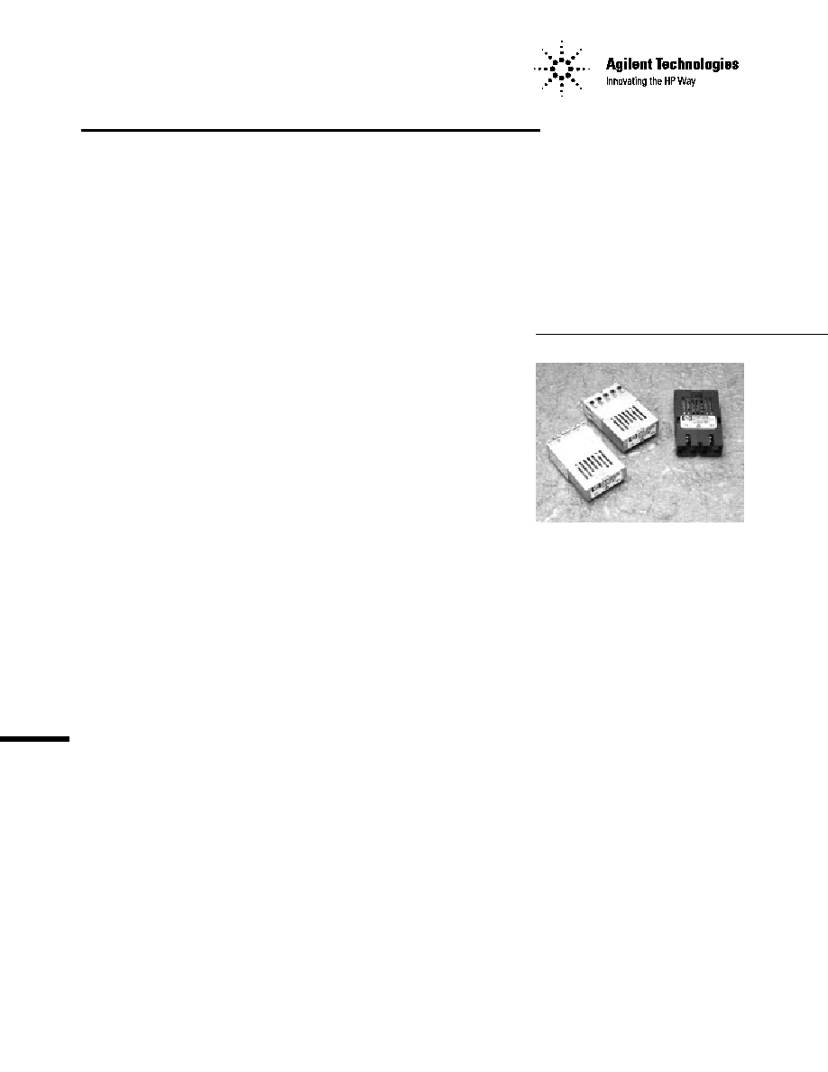
Description
The HFBR/HFCT-53D5
transceiver from Agilent
Technologies allows the system
designer to implement a range of
solutions for multimode and
single mode Gigabit Ethernet
applications.
The overall Agilent transceiver
product consists of three
sections: the transmitter and
receiver optical subassemblies,
an electrical subassembly, and
the package housing which
incorporates a duplex SC
connector receptacle.
Transmitter Section
The transmitter section of the
HFBR-53D5 consists of an
850 nm Vertical Cavity Surface
Emitting Laser (VCSEL) in an
optical subassembly (OSA),
which mates to the fiber cable.
The HFCT-53D5 incorporates a
1300 nm Fabry-Perot (FP) Laser
designed to meet the Gigabit
Ethernet LX specification. The
OSA is driven by a custom,
silicon bipolar IC which converts
differential PECL logic signals
(ECL referenced to a +5 Volt
supply) into an analog laser diode
drive current.

2
Receiver Section
The receiver of the HFBR-53D5
includes a silicon PIN photo-
diode mounted together with a
custom, silicon bipolar
transimpedance preamplifier IC
in an OSA. This OSA is mated to a
custom silicon bipolar circuit that
provides post-amplification and
quantization. The HFCT-53D5
utilizes an InP PIN photodiode in
the same configuration.
The post-amplifier also includes a
Signal Detect circuit which pro-
vides a PECL logic-high output
upon detection of a usable input
optical signal level. This single-
ended PECL output is designed to
drive a standard PECL input
through a 50
PECL load.
Package and Handling
Instructions
Flammability
The HFBR/HFCT-53D5
transceiver housing is made of
high strength, heat resistant,
chemically resistant, and UL
94V-0 flame retardant
plastic.
Recommended Solder and
Wash Process
The HFBR/HFCT-53D5 is
compatible with industry-
standard wave or hand solder
processes.
Process plug
This transceiver is supplied with
a process plug (HFBR-5000) for
protection of the optical ports
within the duplex SC connector
receptacle. This process plug
prevents contamination during
wave solder and aqueous rinse as
well as during handling, shipping
and storage. It is made of a high-
temperature, molded sealing
material that can withstand 80
∞
C
and a rinse pressure of 110 lbs
per square inch.
Recommended Solder fluxes
Solder fluxes used with the
HFBR/HFCT-53D5 should be
water-soluble, organic fluxes.
Recommended solder fluxes
include Lonco 3355-11 from
London Chemical West, Inc. of
Burbank, CA, and 100 Flux from
Alpha-Metals of Jersey City, NJ.
Recommended Cleaning/
Degreasing Chemicals
Alcohols
: methyl, isopropyl,
isobutyl.
Aliphatics
: hexane, heptane
Other:
soap solution, naphtha.
Do not use
partially halogenated
hydrocarbons such as 1,1.1
trichloroethane, ketones such as
MEK, acetone, chloroform, ethyl
acetate, methylene dichloride,
phenol, methylene chloride, or
N-methylpyrolldone. Also, HP
does not recommend the use of
cleaners that use halogenated
hydrocarbons because of their
potential environmental harm.
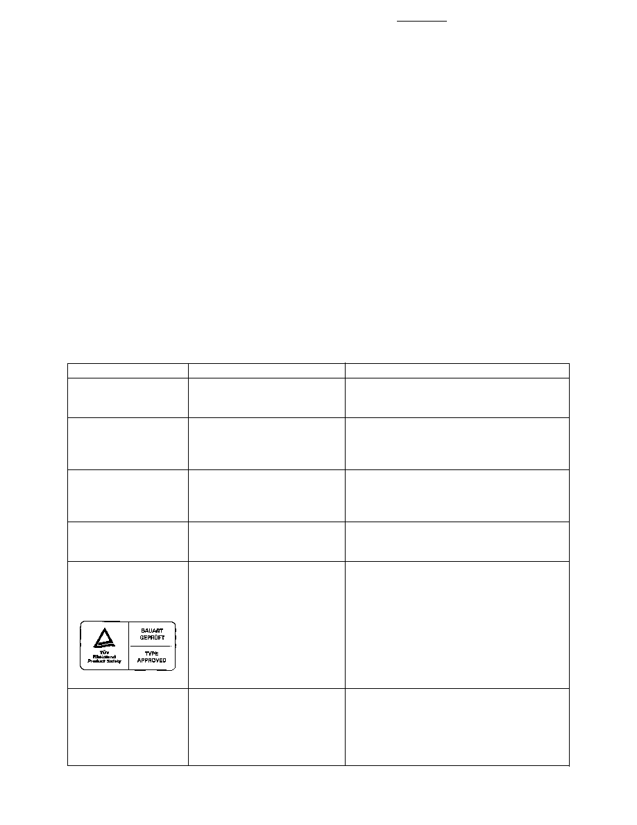
Regulatory Compliance
(See the Regulatory Compliance
Table for transceiver
performance)
The overall equipment design will
determine the certification level.
The transceiver performance is
offered as a figure of merit to
assist the designer in considering
their use in equipment designs.
Electrostatic Discharge (ESD)
There are two design cases in
which immunity to ESD damage
is important.
The first case is during handling
of the transceiver prior to
mounting it on the circuit board.
It is important to use normal ESD
handling precautions for ESD
sensitive devices. These pre-
cautions include using grounded
wrist straps, work benches, and
floor mats in ESD controlled
areas. The transceiver perform-
ance has been shown to provide
adequate performance in typical
industry production
environments.
The second case to consider is
static discharges to the exterior
of the equipment chassis
containing the transceiver parts.
To the extent that the duplex SC
connector receptacle is exposed
to the outside of the equipment
chassis it may be subject to
whatever system-level ESD test
criteria that the equipment is
intended to meet. The transceiver
performance is more robust than
typical industry equipment
requirements of today.
Electromagnetic Interference
(EMI)
Most equipment designs utilizing
these high-speed transceivers
from Agilent will be required to
meet the requirements of FCC in
the United States, CENELEC
EN55022 (CISPR 22) in Europe
and VCCI in Japan. Refer to EMI
section (page 5) for more details.
Immunity
Equipment utilizing these
transceivers will be subject to
radio-frequency electromagnetic
fields in some environments.
These transceivers have good
immunity to such fields due to
their shielded design.
Eye Safety
These laser-based transceivers
are classified as AEL Class I (U.S.
21 CFR(J) and AEL Class 1 per
EN 60825-1 (+A11). They are
eye safe when used within the
data sheet limits per CDRH. They
are also eye safe under normal
operating conditions and under
all reasonably forseeable single
3
fault conditions per EN60825-1.
Agilent has tested the transceiver
design for compliance with the
requirements listed below under
normal operating conditions and
under single fault conditions
where applicable. TUV Rheinland
has granted certi-fication to these
transceivers for laser eye safety
and use in EN 60950 and EN
60825-2 applications. Their
performance enables the
transceivers to be used without
concern for eye safety up to 7
volts transmitter V
CC
.
CAUTION:
There are no user serviceable
parts nor any maintenance
required for the
HFBR/HFCT-53D5. All
adjustments are made at the
factory before shipment to our
customers. Tampering with or
modifying the performance of the
HFBR/HFCT-53D5 will result in
voided product warranty. It may
also result in improper operation
of the HFBR/HFCT-53D5
circuitry, and possible overstress
of the laser source. Device
degradation or product failure
may result.
Regulatory Compliance
Feature
Test Method
Performance
Electrostatic Discharge MIL-STD-883C
Class 1 (>2000 V).
(ESD) to the
Method 3015.4
Electrical Pins
Electrostatic Discharge Variation of IEC 801-2
Typically withstand at least 15 kV without
(ESD) to the
damage when the duplex SC connector
Duplex SC Receptacle
receptacle is contacted by a Human Body
Model probe.
Electromagnetic
FCC Class B
Margins are dependent on customer board and
Interference (EMI)
CENELEC EN55022 Class B
chassis designs.
(CISPR 22A)
VCCI Class I
Immunity
Variation of IEC 801-3
Typically show no measurable effect from a
10 V/m field swept from 27 to 1000 MHz applied
to the transceiver without a chassis enclosure.
Laser Eye Safety
US 21 CFR, Subchapter J
AEL Class I, FDA/CDRH
and Equipment Type
per Paragraphs 1002.10
HFBR-53D5 Accession #9720151- 03
Testing
and 1002.12
HFCT-53D5 Accession #9521220-16
EN 60825-1: 1994 +A11
AEL Class 1, TUV Rheinland of North America
EN 60825-2: 1994
HFBR-53D5:
EN 60950: 1992+A1+A2+A3
Certificate #R9771018.5
Protection Class III
HFCT-53D5:
Certificate 933/51083
Component
Underwriters Laboratories and
UL File E173874 (Pending)
Recognition
Canadian Standards Association
Joint Component Recognition
for Information Technology
Equipment Including Electrical
Business Equipment.
Connection of the HFBR/HFCT-
53D5 to a nonapproved optical
source, operating above the
recommended absolute maximum
conditions or operating the
HFBR/HFCT-53D5 in a manner
inconsistent with its design and
function may result in hazardous
radiation exposure and may be
considered an act of modifying or
manufacturing a laser product.
The person(s) performing such
an act is required by law to
recertify and reidentify the laser
product under the provisions of
U.S. 21 CFR (Subchapter J).

4
Data Line
Interconnections
Agilent Technologies' HFBR/
HFCT-53D5 fiber-optic
transceiver is designed to directly
couple to +5 V PECL signals. The
transmitter inputs are internally
dc-coupled to the laser driver
circuit from the transmitter input
pins (pins 7, 8). There is no
internal, capacitively-coupled 50
Ohm termination resistance
within the transmitter input
section. The transmitter driver
circuit for the laser light source
is a dc-coupled circuit. This
circuit regulates the output
optical power. The regulated light
output will maintain a constant
output optical power provided
the data pattern is reasonably
balanced in duty factor. If the
data duty factor has long, con-
tinuous state times (low or high
data duty factor), then the output
optical power will gradually
change its average output optical
power level to its pre-set value.
As for the receiver section, it is
internally ac-coupled between the
pre-amplifier and the post-
amplifier stages. The actual Data
and Data-bar outputs of the post-
amplifier are dc-coupled to their
respective output pins (pins 2, 3).
Signal Detect is a single-ended,
+5 V PECL output signal that is
dc-coupled to pin 4 of the
module. Signal Detect should not
be ac-coupled externally to the
follow-on circuits because of its
infrequent state changes.
Caution should be taken to
account for the proper intercon-
nection between the supporting
Physical Layer integrated circuits
and this HFBR/HFCT-53D5
transceiver. Figure 3 illustrates a
recommended interface circuit
for interconnecting to a +5 Vdc
PECL fiber-optic transceiver.
APPLICATION SUPPORT
Optical Power Budget
and Link Penalties
The worst-case Optical Power
Budget (OPB) in dB for a fiber-
optic link is determined by the
difference between the minimum
transmitter output optical power
(dBm avg) and the lowest
receiver sensitivity (dBm avg).
This OPB provides the necessary
optical signal range to establish a
working fiber-optic link. The OPB
is allocated for the fiber-optic
cable length and the corre-
sponding link penalties. For
proper link performance, all
penalties that affect the link
performance must be accounted
for within the link optical power
budget. The Gigabit Ethernet
IEEE 802.3z standard identifies,
and has modeled, the
contributions of these OPB
penalties to establish the link
length requirements for 62.5/125
µ
m
and 50/125
µ
m multimode fiber
usage. In addition, single-mode
fiber with standard 1300 nm
Fabry-Perot lasers have been
modeled and specified. Refer to
the IEEE 802.3z standard and its
supplemental documents that
develop the model, empirical
results and final specifications.
10 km Link Support
As well as complying with the LX
5 km standard, the HFCT-53D5
specification provides additional
margin allowing for a 10 km
Gigabit Ethernet link on single
mode fiber. This is accomplished
by limiting the spectral width and
center wavelength range of the
transmitter while increasing the
output optical power and
improving sensitivity. All other
LX cable plant recommendations
should be followed.
Some fiber-optic transceiver sup-
pliers' modules include internal
capacitors, with or without 50 Ohm
termination, to couple their Data
and Data-bar lines to the I/O pins
of their module. When designing
to use these type of transceivers
along with Agilent transceivers, it
is important that the interface
circuit can accommodate either
internal or external capacitive
coupling with 50 Ohm termina-
tion components for proper
operation of both transceiver
designs. The internal dc-coupled
design of the
HFBR/HFCT-53D5 I/O
connections was done to provide
the designer with the most
flexibility for interfacing to
various types of circuits.
Eye Safety Circuit
For an optical transmitter device
to be eye-safe in the event of a
single fault failure, the transmit-
ter must either maintain normal,
eye-safe operation or be disabled.
In the HFBR-53D5 there are
three key elements to the laser
driver safety circuitry: a monitor
diode, a window detector circuit,
and direct control of the laser
bias. The window detection
circuit monitors the average
optical power using the monitor
diode. If a fault occurs such that
the transmitter DC regulation
circuit cannot maintain the preset
bias conditions for the laser
emitter within
±
20%, the
transmitter will automatically be
disabled. Once this has occurred,
only an electrical power reset will
allow an attempted turn-on of the
transmitter.
The HFCT-53D5 utilizes an
integral fiber stub along with a
current limiting circuit to
guarantee eye-safety. It is

5
intrinsically eye safe and does not
require shut down circuitry.
Signal Detect
The Signal Detect circuit provides
a deasserted output signal that
implies the link is open or the
transmitter is OFF as defined by
the Gigabit Ethernet specification
IEEE 802.3z, Table 38.1. The
Signal Detect threshold is set to
transition from a high to low state
between the minimum receiver
input optional power and ≠30 dBm
avg. input optical power
indicating a definite optical fault
(e.g. unplugged connector for the
receiver or transmitter, broken
fiber, or failed far-end transmitter
or data source). A Signal Detect
indicating a working link is
functional when receiving
encoded 8B/10B characters. The
Signal Detect does not detect
receiver data error or error-rate.
Data errors are determined by
Signal processing following the
transceiver.
Electromagnetic
Interference (EMI)
One of a circuit board designer's
foremost concerns is the control
of electromagnetic emissions
from electronic equipment.
Success in controlling generated
Electromagnetic Interference
(EMI) enables the designer to
pass a governmental agency's
EMI regulatory standard; and
more importantly, it reduces the
possibility of interference to
neighboring equipment. There
are three options available for the
HFBR-53D5 and two options for
the HFCT-53D5 with regard to
EMI shielding which provide the
designer with a means to achieve
good EMI performance. The EMI
performance of an enclosure
using these transceivers is
dependent on the chassis design.
Agilent encourages using
standard RF suppression
practices and avoiding poorly
EMI-sealed enclosures.
The first configuration is a
standard HFBR-53D5 fiber-optic
transceiver that has no external
EMI shield. This unit is for
applications where EMI is either
not an issue for the designer, or
the unit resides completely inside
a shielded enclosure, or the
module is used in low density,
extremely quiet applications. The
HFCT-53D5 is not available for
use without an external shield.
The second configuration, option
EM, is for EMI shielding
applications where the position of
the transceiver module will
extend outside the equipment
enclosure. The metallized plastic
package and integral external
metal shield of the transceiver
helps locally to terminate EM
fields to the chassis to prevent
their emissions outside the
enclosure. This metal shield
contacts the panel or enclosure
on the inside of the aperture on
all but the bottom side of the
shield and provides a good RF
connection to the panel. This
option can accommodate various
panel or enclosure thickness, i.e.,
.04 in. min. to 0.10 in. max. The
reference plane for this panel
thickness variation is from the
front surface of the panel or
enclosure. The recommended
length for protruding the
HFBR/HFCT-53D5EM transceiver
beyond the front surface of the
panel or enclosure is 0.25 in.
With this option, there is
flexibility of positioning the
module to fit the specific need of
the enclosure design. (See Figure
6
for the mechanical drawing
dimensions of this shield.)
The third configuration, option
FM, is for applications that are
designed to have a flush
mounting of the module with
respect to the front of the panel
or enclosure. The flush-mount
design accommodates a large
variety of panel thickness, i.e.,
0.04 in. min. to 0.10 in. max.
Note the reference plane for the
flush-mount design is the interior
side of the panel or enclosure.
The recommended distance from
the centerline of the transceiver
front solder posts to the inside
wall of the panel is 0.55 in. This
option contacts the inside panel
or enclosure wall on all four sides
of this metal shield. See Figure 8
for the mechanical drawing
dimensions of this shield.
The two metallized designs are
comparable in their shielding
effectiveness. Both design
options connect only to the
equipment chassis and not to the
signal or logic ground of the
circuit board within the
equipment closure. The front
panel aperture dimensions are
recommended in Figures 7
and 9.
When layout of the printed circuit
board is done to incorporate
these metal-shielded transceivers,
keep the area on the printed
circuit board directly under the
metal shield free of any
components and circuit board
traces. For additional EMI
performance advantage, use
duplex SC fiber-optic connectors
that have low metal content
inside them. This lowers the
ability of the metal fiber-optic
connectors to couple EMI out
through the aperture of the panel
or enclosure.
Evaluation Kit
To help you in your preliminary
transceiver evaluation, Agilent
offers a 1250 MBd Gigabit