 | –≠–ª–µ–∫—Ç—Ä–æ–Ω–Ω—ã–π –∫–æ–º–ø–æ–Ω–µ–Ω—Ç: HFBR-5527 | –°–∫–∞—á–∞—Ç—å:  PDF PDF  ZIP ZIP |
Document Outline
- List of Figures
- 1. Transmitter and Receiver Application Circuit with +5 V ECL Inputs and Outputs.
- 2. Recommended Power Supply Filter and +5 V ECL Signal Terminations for the Transmitter and Receiver Application Circuit of Figu
- 3. Average Modulated Power.
- 4. Typical Optical Power Budget vs. Data Rate
- 5. Test Circuit for Measuring Unpeaked Rise and Fall Times
- 6. Typical Spectra Normalized to the 25∞C Peak
- 7. Typical Forward Voltage vs. Drive Current.
- 8. Typical Normalized Output Optical Power vs. Drive Current with the Drive Circuit in Figure 1 Recommended Application Circuit
- 9. Recommended Power Supply Filter Circuit.
- 10. Simplified Receiver Schematic.
- 11. Typical Pulse Width Distortion vs. Peak Input Power
- 12. Typical Output Spectral Noise Density vs. Frequency
- 13. Typical Rise and Fall Time vs. Temperature
- Features
- Applications
- Description
- HFBR-5527 125 MBd Data Link
- Recommended Operating Conditions for the Circuits in Figures 1 and 2.
- Link Performance
- Plastic Optical Fiber (1 mm POF) Transmitter Application Circuit
- Hard Clad Silica Fiber (200 mm HCS) Transmitter Application Circuit
- Plastic and Hard Clad Silica Optical Fiber Receiver Application Circuit
- 125 Megabaud Fiber Optic Link Transmitter/Receiver
- Description
- Absolute Maximum Ratings
- HFBR-5527 Transmitter Electrical/Optical Characteristics
- HFBR-5527 Receiver Electrical/Optical Characteristics
- HFBR-5527 Mechanical Dimensions
- Printed Circuit Board Layout Dimensions
165
125 Megabaud Fiber Optic
Transceiver
JIS FO7 Connection
Technical Data
Features
∑ Data Transmission at Signal
Rates of 1 to 125 MBd over
Distances up to 100 Meters
∑ Compatible with Duplex JIS
FO7 and Simplex JIS FO5
Connectors
∑ Specified for Use with
Plastic Optical Fiber (POF),
and with Large Core Silica
Fiber (HCS
Æ
)
∑ Transmitter and Receiver
Application Circuit
Schematics Available
∑ Conductive Plastic Housing
Provides Electrical Shield
Applications
∑ Intra-System Links: Board-
to-Board, Rack-to-Rack
∑ High Voltage Isolation
∑ Telecommunications
Switching Systems
∑ Computer-to-Peripheral Data
Links, PC Bus Extension
∑ Industrial Control Networks
∑ Proprietary LANs
∑ Digitized Video
∑ Medical Instruments
∑ Immune to Lightning and
Voltage Transients
Description
The 125 MBd transceiver is a
cost-effective fiber-optic solution
for transmission of 125 MBd data
up to 100 meters with HCS
Æ
fiber. The data link consists of a
650 nm visible, red LED trans-
mitter and a PIN/preamp receiver.
These can be used with low-cost
plastic or hard clad silica fiber.
One millimeter diameter plastic
fiber provides the lowest cost
solution for distances under 25
meters. The lower attenuation of
HCS
Æ
fiber allows data transmis-
sion over longer distance. These
components can be used for high
speed data links without the
problems common with copper
wire solutions.
The transmitter is a high power
650 nm LED. Both transmitter
and receiver are molded in one
housing which is compatible with
the FO7 connector. This con-
nector is designed to efficiently
couple the power into POF or
HCS
Æ
fiber.
HFBR-5527
With the recommended drive
circuit, the LED operates at
speeds from 1-125 MBd. The
analog high bandwidth receiver
contains a PIN photodiode and
internal transimpedance
amplifier. With the recommended
application circuit for 125 MBd
operation, the performance of the
complete data link is specified for
0-25 meters with plastic fiber. A
wide variety of other digitizing
circuits can be combined with the
HFBR-5527 Series to optimize
performance and cost at higher or
lower data rates.
HCS
Æ
is a registered trademark of Spectran Corporation.
5965-7092E (5/97)
166
HFBR-5527
125 MBd Data Link
Data link operating conditions
and performance are specified for
the transmitter and receiver in
the recommended applications
circuits shown in Figure 1. This
circuit has been optimized for
125 MBd operation. The
Applications Engineering
Department in the Hewlett-
Recommended Operating Conditions for the Circuits in Figures 1 and 2.
Parameter
Symbol
Min.
Max.
Unit
Note
Ambient Temperature
T
A
0
70
∞
C
Supply Voltage
V
CC
+4.75
+5.25
V
Data Input Voltage - Low
V
IL
V
CC
≠1.89
V
CC
≠1.62
V
Data Input Voltage - High
V
IH
V
CC
≠1.06
V
CC
≠0.70
V
Data Output Load
R
L
45
55
1
Signaling Rate
f
S
1
125
MBd
Duty Cycle
D.C.
40
60
%
2
Link Performance
: 1-125 MBd, BER
10
-9
, under recommended operating conditions with
recommended transmit and receive application circuits.
Parameter
Symbol
Min.
[3]
Typ.
[4]
Max.
Unit
Condition
Note
Optical Power Budget, 1 m POF
OPB
POF
11
16
dB
5, 6, 7
Optical Power Margin,
OPM
POF,20
3
6
dB
5, 6, 7
20 m Standard POF
Link Distance with
1
20
27
m
Standard 1 mm POF
Optical Power Margin,
OPM
POF,25
3
6
dB
5, 6, 7
25 m Low Loss POF
Link Distance with Extra
1
25
32
m
Low Loss 1 mm POF
Optical Power Budget, 1 m HCS
OPB
HCS
12
dB
5, 6, 7
Optical Power Margin, 100 m HCS
OPM
HCS,100
6
dB
5, 6, 7
Link Distance with HCS cable
1
125
m
Notes:
1. If the output of U4C in Figure 1, page 4 is transmitted via coaxial cable, terminate with a 50
resistor to V
CC
- 2 V.
2. Run length limited code with maximum run length of 10
µ
s.
3. Minimum link performance is projected based on the worst case specifications of the transmitter, receiver, and POF cable, and the
typical performance of other components (e.g., logic gates, transistors, resistors, capacitors, quantizer, HCS cable).
4. Typical performance is at 25
∞
C, 125 MBd, and is measured with typical values of all circuit components.
5. Standard cable is HFBR-RXXYYY plastic optical fiber, with a maximum attenuation of 0.24 dB/m at 650 nm and NA = 0.5.
Extra low loss cable is HFBR-EXXYYY plastic optical fiber, with a maximum attenuation of 0.19 dB/m at 650 nm and NA = 0.5.
HCS cable is HFBR-H/VXXYYY glass optical fiber, with a maximum attenuation of 10 dB/km at 650 nm and NA = 0.37.
6. Optical Power Budget is the difference between the transmitter output power and the receiver sensitivity, measured after
1 meter of fiber. The minimum OPB is based on the limits of optical component performance over temperature, process, and
recommended power supply variation.
7. The Optical Power Margin is the available OPB after including the effects of attenuation and modal dispersion for the minimum
link distance: OPM = OPB - (attenuation power loss + modal dispersion power penalty). The minimum OPM is the margin
available for long term LED LOP degradation and additional fixed passive losses (such as in-line connectors) in addition to the
minimum specified distance.
Packard Optical Communication
Division is available to assist in
optimizing link performance for
higher or lower speed operation.
167
Hard Clad Silica Fiber (200
µ
m HCS) Transmitter Application Circuit:
Performance of
the transmitter in the recommended application circuit (Figure 1) for HCS; 1-125 MBd, 25
∞
C.
Parameter
Symbol
Typical
Unit
Condition
Note
Average Optical Power 200
µ
m HCS
P
avg
-14.6
dBm
50% Duty
Note 1, Fig. 3
Cycle
Average Modulated Power 200
µ
m HCS
P
mod
-16.2
dBm
Note 2, Fig. 3
Optical Rise Time (10% to 90%)
t
r
3.1
ns
5 MHz
Optical Fall Time (90% to 10%)
t
f
3.4
ns
5 MHz
High Level LED Current (On)
I
F,H
60
mA
Note 3
Low Level LED Current (Off)
I
F,L
6
mA
Note 3
Optical Overshoot - 200
µ
m HCS
30
%
Transmitter Application Circuit
I
CC
130
mA
Figure 1
Current Consumption - 200
µ
m HCS
Notes:
1. Average optical power is measured with an average power meter at 50% duty cycle, after 1 meter of fiber.
2. To allow the LED to switch at high speeds, the recommended drive circuit modulates LED light output between two non-zero power
levels. The modulated (useful) power is the difference between the high and low level of light output power (transmitted) or input
power (received), which can be measured with an average power meter as a function of duty cycle (see Figure 3). Average Modulated
Power is defined as one half the slope of the average power versus duty cycle:
[P
avg
@ 80% duty cycle - P
avg
@ 20% duty cycle]
Average Modulated Power = ≠≠--------------------------------------------
(2) [0.80 - 0.20]
3. High and low level LED currents refer to the current through the LED. The low level LED "off" current, sometimes referred to as
"hold-on" current, is prebias supplied to the LED during the off state to facilitate fast switching speeds.
Plastic Optical Fiber (1 mm POF) Transmitter Application Circuit:
Performance of the transmitter in the recommended application circuit (Figure 1) for POF; 1-125 MBd, 25
∞
C.
Parameter
Symbol
Typical
Unit
Condition
Note
Average Optical Power 1 mm POF
P
avg
-9.7
dBm
50% Duty
Note 1, Fig. 3
Cycle
Average Modulated Power 1 mm POF
P
mod
-11.3
dBm
Note 2, Fig. 3
Optical Rise Time (10% to 90%)
t
r
2.1
ns
5 MHz
Optical Fall Time (90% to 10%)
t
f
2.8
ns
5 MHz
High Level LED Current (On)
I
F,H
30
mA
Note 3
Low Level LED Current (Off)
I
F,L
3
mA
Note 3
Optical Overshoot - 1 mm POF
45
%
Transmitter Application Circuit
I
CC
115
mA
Figure 1
Current Consumption - 1 mm POF
168
Plastic and Hard Clad Silica Optical Fiber Receiver Application Circuit:
Performance
[4]
of the receiver in the recommended application circuit (Figure 1); 1-125 MBd, 25
∞
C unless
otherwise stated.
Parameter
Symbol
Typical
Unit
Condition
Note
Data Output Voltage - Low
V
OL
V
CC
-1.7
V
R
L
= 50
Note 5
Data Output Voltage - High
V
OH
V
CC
-0.9
V
R
L
= 50
Note 5
Receiver Sensitivity to Average
P
min
-27.5
dBm
50% eye opening
Note 2
Modulated Optical Power 1 mm POF
Receiver Sensitivity to Average
P
min
-28.5
dBm
50% eye opening
Note 2
Modulated Optical Power 200
µ
m HCS
Receiver Overdrive Level of Average
P
max
-7.5
dBm
50% eye opening
Note 2
Modulated Optical Power 1 mm POF
Receiver Overdrive Level of Average
P
max
-10.5
dBm
50% eye opening
Note 2
Modulated Optical Power 200
µ
m HCS
Receiver Application Circuit Current
I
CC
85
mA
R
L
=
Figure 1
Consumption
Notes:
4. Performance in response to a signal from the transmitter driven with the recommended circuit at 1-125 MBd over 1 meter of plastic
optical fiber or 1 meter of HCS
Æ
fiber with F07 plugs.
5. Terminated through a 50
resistor to V
CC
- 2 V.
6. If there is no input optical power to the receiver, electrical noise can result in false triggering of the receiver. In typical applications,
data encoding and error detection prevent random triggering from being interpreted as valid data.
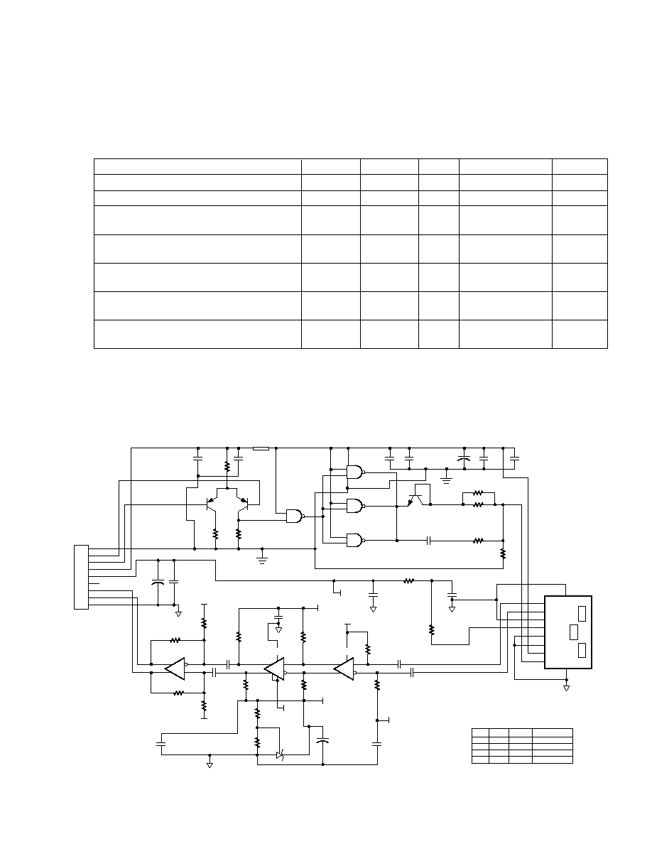
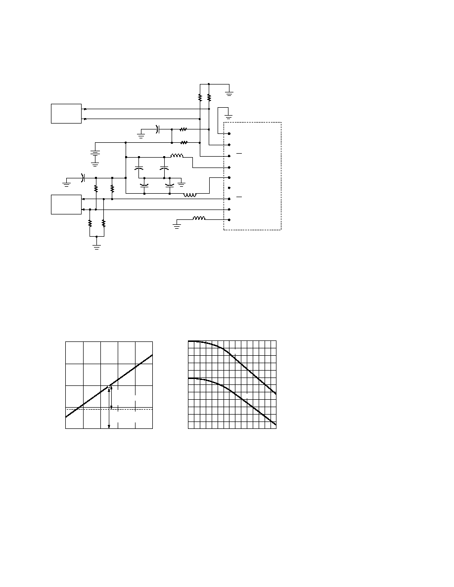
Figure 1. Transmitter and Receiver Application Circuit with +5 V ECL Inputs and Outputs.
C1
0.001
C2
0.1
R5
22
Q1
MPS536L
R6
91
R7
91
Q2
MPS536L
C20
10
C19
0.1
T
X
V
EE
9
8
7
6
5
4
3
2
1
J1
Q2 BASE
Q1 BASE
T
X
V
CC
R
X
V
CC
PIN 19 10H116
PIN 18 10H116
R
X
V
EE
NC
L1
CB70-1812
1
2
3
4
5
13
12
10
9
14
7
8
11
6
2
3
4
12
13
5
7
8
9
3
4
17
15
19
18
R24
1K
R22
1K
R18
51
R16
51
C17
0.1
V
BB
V
CC
C10
0.1
R19
51
R17
51
R15
1K
R23
1K
V
BB
C18
0.1
R25
1K
R20
12
R21
62
V
CC
V
BB
3 V
C14
10
TL431
U5
MC10H116FN
C15
0.1
C11
0.1
C16
0.1
C12
0.1
R14
1K
V
BB
3V
C9
47
R12
4.7
C13
0.1
R13
4.7
U4C
U4A
U4B
R11*
R10
15
C8*
74ACTQ00
U1B
74ACTQ00
U1D
74ACTQ00
U1C
R9*
R8*
C7
0.001
C6
0.1
C5
10
C4
0.001
C3
0.1
Q3
2N3904
V
CC
74ACTQ00
U1A
POF
180
180
820
62 pF
R8
R9
R11
C8
HCS
82
82
470
120 pF
TOLERANCE
1%
1%
1%
5%
THE VALUES OF R8, R9, R11, AND
C8 ARE DIFFERENT FOR POF AND
HCS DRIVE CIRCUITS.
UNLESS OTHERWISE NOTED,
ALL CAPACITOR VALUES
ARE IN µF WITH ± 10%
TOLERANCE AND ALL
RESISTOR VALUES ARE IN
WITH ± 5% TOLERANCE.
MC10H116FN
MC10H116FN
2
20
+
+
+
10
14
RX GND
5
8
7
6
9
10
U22
RX GND
RX GND
RX V
CC
GND
GND
ANODE
CATHODE
RX OUT
1
169
Figure 2. Recommended Power Supply Filter and +5 V ECL Signal Terminations
for the Transmitter and Receiver Application Circuit of Figure 1.
Figure 4. Typical Optical Power
Budget vs. Data Rate.
Figure 3. Average Modulated Power.
OPTICAL POWER BUDGET ≠dB
10
21
15
9
DATA RATE ≠ MBd
90
70
130
150
19
11
110
17
13
30
50
POF
HCS
8 TD
9 T
X
V
EE
7 TD
6 T
X
V
CC
5 R
X
V
CC
4
3 RD
2 RD
82
10 µF
0.1 µF
4.7 µH
0.1 µF
1 R
X
V
EE
+5 V ECL
SERIAL DATA
SOURCE
0.1 µF
0.1 µF
82
120
120
+5 V ECL
SERIAL DATA
RECEIVER
4.7 µH
10 µF
+
+
+
≠
5 V
82
82
120
120
FIBER-OPTIC
TRANSCEIVER
SHOWN IN
FIGURE 1
4.7 µH
AVERAGE POWER ≠ µW
0
200
100
0
DUTY CYCLE ≠ %
20
40
80
100
150
50
60
AVERAGE POWER,
50% DUTY CYCLE
AVERAGE
MODULATED
POWER