 | –≠–ª–µ–∫—Ç—Ä–æ–Ω–Ω—ã–π –∫–æ–º–ø–æ–Ω–µ–Ω—Ç: HFBR-5803 | –°–∫–∞—á–∞—Ç—å:  PDF PDF  ZIP ZIP |
HFBR-5803/5803T/5803A/5803AT
FDDI, 100 Mb/s ATM, and Fast Ethernet
Transceivers in Low Cost 1 x 9 Package
Style
Data Sheet
Description
The HFBR-5800 family of trans-
ceivers from Agilent provide the
system designer with products
to implement a range of Fast
Ethernet, FDDI and ATM
(Asynchronous Transfer Mode)
designs at the 100 Mb/s-125
MBd rate.
The transceivers are all supplied
in the industry standard 1 x 9
SIP package style with either a
duplex SC or a duplex ST*
connector interface.
FDDI PMD, ATM and Fast Ethernet
2 km Backbone Links
The HFBR-5803/5803T are
1300 nm products with optical
performance compliant with the
FDDI PMD standard. The FDDI
PMD standard is ISO/IEC
9314-3:
1990 and ANSI X3.166 - 1990.
These transceivers for 2 km
multimode fiber backbones are
supplied in the small 1 x 9
duplex SC or ST package style.
The HFBR-5803/-5803T is useful
for both ATM 100 Mb/s
interfaces and Fast Ethernet 100
Base-FX interfaces. The ATM
Forum User-Network Interface
(UNI) Standard, Version 3.0,
defines the Physical Layer for
100 Mb/s Multimode Fiber
Interface for ATM in Section 2.3
to be the FDDI PMD Standard.
Features
∑ Full compliance with the optical
performance requirements of the
FDDI PMD standard
∑ Full compliance with the FDDI
LCF-PMD standard
∑ Full compliance with the optical
performance requirements of the
ATM 100 Mb/s physical layer
∑ Full compliance with the optical
performance requirements of
100 Base-FX version of IEEE 802.3u
∑ Multisourced 1 x 9 package style
with choice of duplex SC or
duplex ST* receptacle
∑ Wave solder and aqueous wash
process compatible
∑ Manufactured in an ISO 9002
certified facility
∑ Single +3.3 V or +5 V power
supply
Applications
∑ Multimode fiber backbone links
∑ Multimode fiber wiring closet to
desktop links
∑ Very low cost multimode fiber
links from wiring closet to
desktop
∑ Multimode fiber media converters
*ST is a registered trademark of AT&T
Lightguide Cable Connectors.
Note: The "T" in the product numbers
indicates a transceiver with a duplex ST
connector receptacle.
Product numbers without a "T" indicate
transceivers with a duplex SC connector
receptacle.
Likewise, the Fast Ethernet
Alliance defines the Physical
Layer for 100 Base-FX for Fast
Ethernet to be the FDDI PMD
Standard.
ATM applications for physical
layers other than 100 Mb/s
Multimode Fiber Interface are
supported by Agilent. Products
are available for both the single
mode and the multimode fiber
SONET OC-3c (STS-3c) ATM
interfaces and the 155 Mb/s-194
MBd multimode fiber ATM
interface as specified in the ATM
Forum UNI.
Contact your Agilent sales
representative for information
on these alternative Fast
Ethernet, FDDI and ATM
products.
Ordering Information
The HFBR-5803/5803T/5803A/
5803AT 1300 nm products are
available for production orders
through the Agilent Component
Field Sales Offices and
Authorized Distributors world
wide.
0 ∞C to +70 ∞C
HFBR-5803/5803T
-10 ∞C TO +85 ∞C
HFBR-5803A/5803AT
2
Transmitter Sections
The transmitter section of the
HFBR-5803 and HFBR-5805
series utilize 1300 nm Surface
Emitting InGaAsP LEDs. These
LEDs are packaged in the optical
subassembly portion of the
transmitter section. They are
driven by a custom silicon IC
which converts differential
PECL logic signals, ECL
referenced (shifted) to a +3.3 V
or +5 V supply, into an analog
LED drive current.
Receiver Sections
The receiver sections of the
HFBR-5803 and HFBR-5805
series utilize InGaAs PIN photo-
diodes coupled to a custom
silicon transimpedance
preamplifier IC. These are
packaged in the optical sub-
assembly portion of the receiver.
These PIN/preamplifier combi-
nations are coupled to a custom
quantizer IC which provides the
final pulse shaping for the logic
output and the Signal Detect
function. The data output is dif-
ferential. The signal detect
output is single-ended. Both
data and signal detect outputs
are PECL compatible, ECL
referenced (shifted) to a +3.3 V
or +5 V power supply.
Package
The overall package concept for
the Agilent transceivers consists
of the following basic elements;
two optical subassemblies, an
electrical subassembly and the
housing as illustrated in Figure 1
and Figure 1a.
The package outline drawings
and pin out are shown in
Figures 2, 2a and 3. The details
of this package outline and pin
out are compliant with the
multisource definition of the 1 x
9 SIP. The low profile of the
Agilent transceiver design
complies with the maximum
height allowed for the duplex SC
connector over the entire length
of the package.
The optical subassemblies utilize
a high volume assembly process
together with low cost lens
elements which result in a cost
effective building block.
The electrical subassembly con-
sists of a high volume multilayer
printed circuit board on which
the IC chips and various surface-
mounted passive circuit
elements are attached.
The package includes internal
shields for the electrical and
optical subassemblies to ensure
low EMI emissions and high
immunity to external EMI fields.
The outer housing including the
duplex SC connector receptacle
or the duplex ST ports is molded
of filled nonconductive plastic to
provide mechanical strength and
electrical isolation. The solder
posts of the Agilent design are
isolated from the circuit design
of the transceiver and do not
require connection to a ground
plane on the circuit board.
The transceiver is attached to a
printed circuit board with the
nine signal pins and the two
solder posts which exit the
bottom of the housing. The two
solder posts provide the primary
mechanical strength to
withstand the loads imposed on
the transceiver by mating with
duplex or simplex SC or ST
connectored fiber cables.
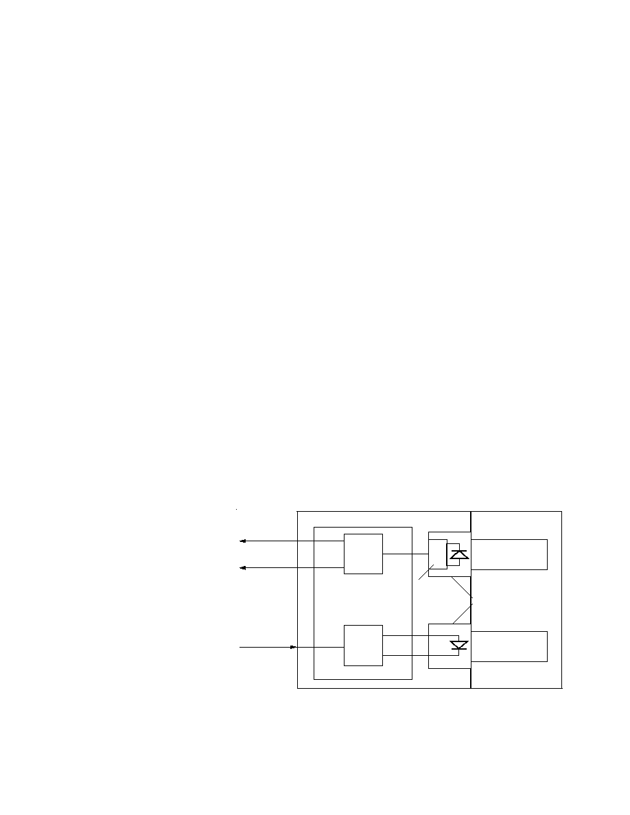
Figure 1. SC Connector Block Diagram.
TOP VIEW
PIN PHOTODIODE
DUPLEX SC
RECEPTACLE
OPTICAL
SUBASSEMBLIES
LED
PREAMP IC
DATA OUT
SIGNAL
DETECT OUT
DATA IN
ELECTRICAL SUBASSEMBLY
QUANTIZER IC
DRIVER IC
DIFFERENTIAL
SINGLE-ENDED
DIFFERENTIAL
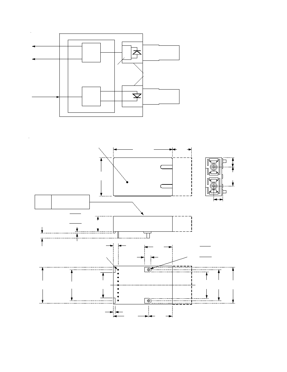
3
DATA OUT
SIGNAL
DETECT OUT
DATA IN
ELECTRICAL SUBASSEMBLY
QUANTIZER IC
DRIVER IC
TOP VIEW
PIN PHOTODIODE
DUPLEX ST
RECEPTACLE
OPTICAL
SUBASSEMBLIES
LED
PREAMP IC
DIFFERENTIAL
SINGLE-ENDED
DIFFERENTIAL
Figure 1a. ST Connector Block Diagram.
Figure 2. SC Connector Package Outline Drawing with standard height.
39.12
(1.540)
MAX.
AREA
RESERVED
FOR
PROCESS
PLUG
12.70
(0.500)
25.40
(1.000)
MAX.
12.70
(0.500)
10.35
(0.407)
MAX.
3.30 ± 0.38
(0.130 ± 0.015)
HFBR-5803
DATE CODE (YYWW)
SINGAPORE
2.92
(0.115)
20.32
(0.800)
[8x(2.54/.100)]
23.55
(0.927)
16.70
(0.657)
0.46
(0.018)
NOTE 1
(9x)
ÿ
NOTE 1
0.87
(0.034)
23.24
(0.915)
15.88
(0.625)
NOTE 1: THE SOLDER POSTS AND ELECTRICAL PINS ARE PHOSPHOR BRONZE WITH TIN LEAD OVER NICKEL PLATING.
DIMENSIONS ARE IN MILLIMETERS (INCHES).
+ 0.08
≠ 0.05
+ 0.003
≠ 0.002
0.75
(0.030
)
)
6.35
(0.250)
5.93 ± 0.1
(0.233 ± 0.004)
AGILENT
20.32
(0.800)
17.32
(0.682
23.32
(0.918)
18.52
(0.729)
4.14
(0.163
+ 0.25
≠ 0.05
+ 0.010
≠ 0.002
1.27
(0.050
Case Temperature
Measurement Point
4
Figure 2a. ST Connector Package Outline Drawing with standard height.
Figure 3. Pin Out Diagram.
1 = V
EE
2 = RD
3 = RD
4 = SD
5 = V
CC
6 = V
CC
7 = TD
8 = TD
9 = V
EE
TOP VIEW
N/C
N/C
Rx
Tx
25.4
(1.000)
MAX.
24.8
(0.976)
42
(1.654)
MAX.
5.99
(0.236)
12.7
(0.500)
12.0
(0.471)
MAX.
0.5
(0.020)
3.3 ± 0.38
(0.130 ± 0.015)
+ 0.08
- 0.05
+ 0.003
- 0.002
+ 0.25
- 0.05
+ 0.010
- 0.002
20.32
± 0.38
(± 0.015)
HFBR-5803T
DATE CODE (YYWW)
SINGAPORE
3.2
(0.126)
2.6
(0.102)
ÿ
22.86
(0.900)
20.32
(0.800)
[(8x (2.54/0.100)]
17.4
(0.685)
21.4
(0.843)
20.32
(0.800)
3.6
(0.142)
1.3
(0.051)
23.38
(0.921)
18.62
(0.733)
NOTE 1: PHOSPHOR BRONZE IS THE BASE MATERIAL FOR THE POSTS & PINS WITH TIN LEAD OVER NICKEL PLATING.
DIMENSIONS IN MILLIMETERS (INCHES).
(
(
( )
0.46
(0.018)
NOTE 1
ÿ
1.27
(0.050)
Case Temperature
Measurement Point
5
Application Information
The Applications Engineering
group in the Agilent Fiber Optics
Communication Division is
available to assist you with the
technical understanding and
design trade-offs associated with
these transceivers. You can
contact them through your
Agilent sales representative.
The following information is
provided to answer some of the
most common questions about
the use of these parts.
Transceiver Optical Power Budget
versus Link Length
Optical Power Budget (OPB) is
the available optical power for a
fiber optic link to accommodate
fiber cable losses plus losses due
to in-line connectors, splices,
optical switches, and to provide
margin for link aging and
unplanned losses due to cable
plant reconfiguration or repair.
Figure 4 illustrates the predicted
OPB associated with the
transceiver series specified in
this data sheet at the Beginning
of Life (BOL). These curves
represent the attenuation and
chromatic plus modal dispersion
losses associated with the 62.5/
125 µm and 50/125 µm fiber
cables only. The area under the
curves represents the remaining
OPB at any link length, which is
available for overcoming non-
fiber cable related losses.
Agilent LED technology has
produced 1300 nm LED devices
with lower aging characteristics
than normally associated with
these technologies in the
industry. The industry conven-
tion is 1.5 dB aging for 1300 nm
LEDs. The Agilent 1300 nm
LEDs will experience less than
1 dB of aging over normal com-
mercial equipment mission life
periods. Contact your Agilent
sales representative for
additional details.
Figure 4 was generated with a
Agilent fiber optic link model
containing the current industry
conventions for fiber cable
specifications and the FDDI
PMD and LCF-PMD optical
parameters. These parameters
are reflected in the guaranteed
performance of the transceiver
specifications in this data sheet.
This same model has been used
extensively in the ANSI and
IEEE committees, including the
ANSI X3T9.5 committee, to
establish the optical performance
requirements for various fiber
optic interface standards. The
cable parameters used come
from the ISO/IEC JTC1/SC 25/
WG3 Generic Cabling for
Customer Premises per
DIS 11801 document and the
EIA/TIA-568-A Commercial
Building Telecommunications
Cabling Standard per SP-2840.
Figure 4. Optical Power Budget at BOL versus
Fiber Optic Cable Length.
Transceiver Signaling Operating
Rate Range and BER Performance
For purposes of definition, the
symbol (Baud) rate, also called
signaling rate, is the reciprocal
of the shortest symbol time. Data
rate (bits/sec) is the symbol rate
divided by the encoding factor
used to encode the data
(symbols/bit).
When used in Fast Ethernet,
FDDI and ATM 100 Mb/s
applications the performance of
the 1300 nm transceivers is
guaranteed over the signaling
rate of 10 MBd to
125 MBd to the full conditions
listed in individual product
specification tables.
Figure 5. Transceiver Relative Optical Power
Budget at Constant BER vs. Signaling Rate.
The transceivers may be used
for other applications at signal-
ing rates outside of the 10 MBd
to 125 MBd range with some
penalty in the link optical power
budget primarily caused by a
reduction of receiver sensitivity.
Figure 5 gives an indication of
the typical performance of these
1300 nm products at different
rates.
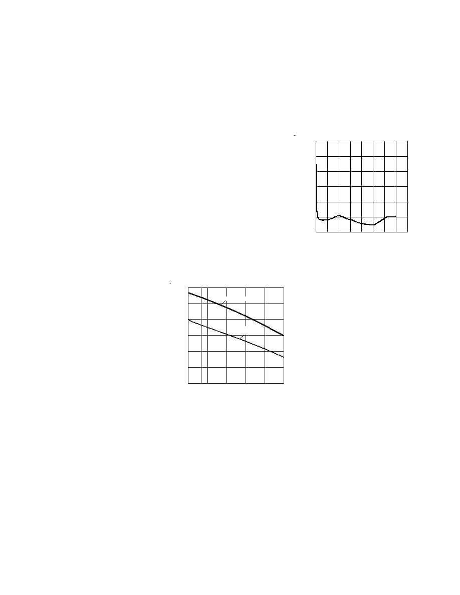
These transceivers can also be
used for applications which
require different Bit Error Rate
(BER) performance. Figure 6
illustrates the typical trade-off
between link BER and the
receivers input optical power
level.
OP
T
I
CA
L
P
O
WE
R
BU
D
G
E
T
(d
B)
0
FIBER OPTIC CABLE LENGTH (km)
0.5
1.5
2.0
2.5
12
10
8
6
4
2
1.0
0.3
HFBR-5803, 62.5/125 µm
HFBR-5803
50/125 µm
TR
A
N
S
C
EI
VER
R
E
L
A
TI
VE O
P
TI
C
A
L
PO
W
E
R
B
U
D
G
ET
A
T
CONS
T
A
NT
B
E
R
(
d
B
)
0
200
0
SIGNAL RATE (MBd)
25
75
100
125
2.5
2.0
1.5
1.0
175
0.5
50
150
CONDITIONS:
1. PRBS 2
7
-1
2. DATA SAMPLED AT CENTER OF DATA SYMBOL.
3. BER = 10
-6
4. T
A
= +25∞ C
5. V
CC
= 3.3 V to 5 V dc
6. INPUT OPTICAL RISE/FALL TIMES = 1.0/2.1 ns.
0.5