Hfct5205.p65
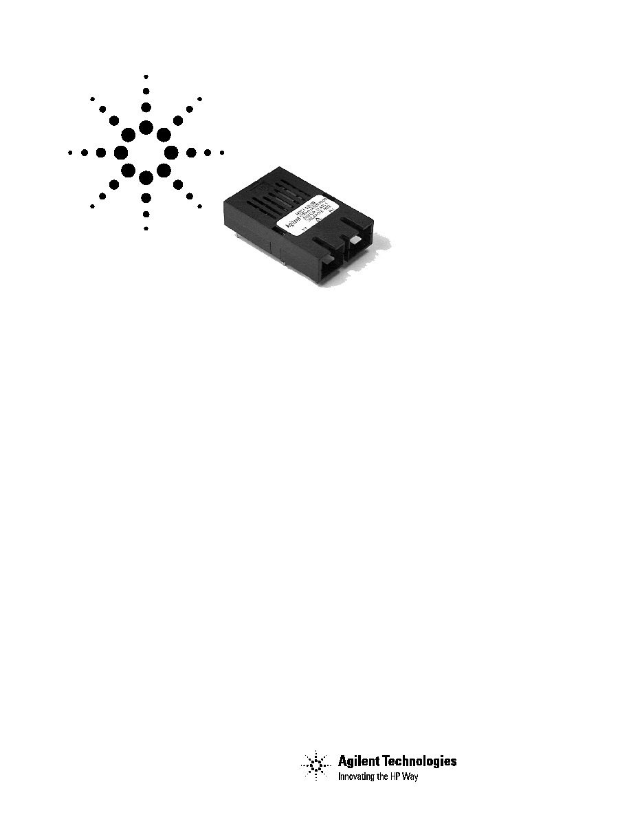
Agilent HFCT-5205 SC Duplex
Single Mode Transceiver
Data Sheet
Description
The HFCT-5205 transceiver is a
high performance, cost effective
module for serial optical data
communications applications
specified for a signal rate of
155 MBd. It is designed to provide
a SONET/SDH compliant link for
155 Mb/s intermediate reach links.
This module is designed for single
mode fiber and operates at a
nominal wavelength of 1300 nm.
It incorporates Agilent's high
performance, reliable, long
wavelength optical devices and
proven circuit technology to give
long life and consistent service.
The transmitter section uses a
Multiple Quantum Well laser with
full IEC 825 and CDRH Class I eye
safety.
The receiver section uses a planar
PIN photodetector for low dark
current and excellent
responsivity.
A pseudo-ECL logic interface
simplifies interface to external
circuitry.
Features
· SC duplex single mode
transceiver
· Intermediate SONET OC3 SDH
STM1 (S1.1) compliant
· Single +5 V power supply
· Multisourced 1 x 9 pin
configuration
· Aqueous washable plastic
package
· Interchangeable with LED
multisourced 1 x 9 transceivers
· Unconditionally eye safe laser IEC
825/CDRH Class 1 compliant
· Two temperature ranges:
0°C to +70°C - HFCT-5205B/D
-40°C to +85°C - HFCT-5205A/C
Applications
· SONET/SDH equipment
interconnect
· ATM 155 Mb/s links

2
Connection Diagram
Pin Descriptions:
Pin 1 Receiver Signal Ground V
EER
:
Directly connect this pin to the
receiver ground plane.
Pin 2 Receiver Data Out RD:
See recommended circuit
schematic, Figure 4.
Pin 3 Receiver Data Out Bar RD:
See recommended circuit
schematic, Figure 4.
Pin 4 Signal Detect SD:
Normal optical input levels to the
receiver result in a logic "1"
output.
Low optical input levels to the
receiver result in a fault condition
indicated by a logic "0" output.
This Signal Detect output can be
used to drive a PECL input on an
upstream circuit, such as Signal
Detect input or Loss of Signal-bar.
Pin 5 Receiver Power Supply V
CCR
:
Provide +5 V dc via the
recommended transmitter power
supply filter circuit. Locate the
power supply filter circuit as close
as possible to the V
CC
pin.
Pin 6 Transmitter Power Supply V
CCT
:
Provide +5 V dc via the
recommended transmitter power
supply filter circuit. Locate the
power supply filter circuit as close
as possible to the V
CC
pin.
Pin 7 Transmitter Data In Bar TD:
See recommended circuit
schematic, Figure 4.
Pin 8 Transmitter Data In TD:
See recommended circuit
schematic, Figure 4.
Pin 9 Transmitter Signal Ground V
EET
:
Directly connect this pin to the
transmitter ground plane.
Mounting Studs
The mounting studs are provided
for mechanical attachment to the
circuit board. They are embedded
in the nonconductive plastic
housing and are not tied to the
transceiver internal circuit and
should be soldered into
plated-through holes on the
printed circuit board.
RECEIVER SIGNAL GROUND
RECEIVER DATA OUT
RECEIVER DATA OUT BAR
SIGNAL DETECT
RECEIVER POWER SUPPLY
TRANSMITTER POWER SUPPLY
TRANSMITTER DATA IN BAR
TRANSMITTER DATA IN
TRANSMITTER SIGNAL GROUND
o
o
o
o
o
o
o
o
o
1
2
3
4
5
6
7
8
9
Top View
N/C
N/C
3
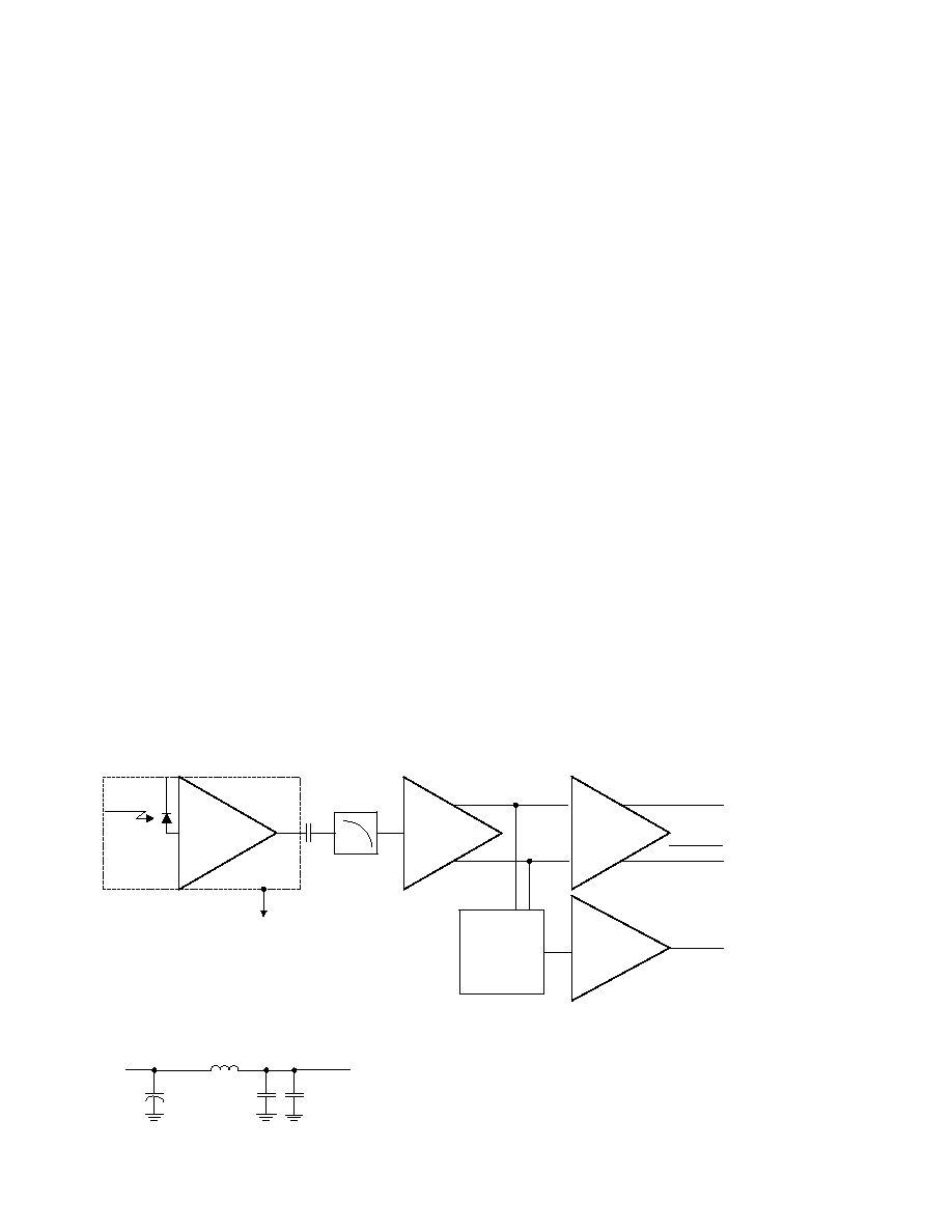
Functional Description
Receiver Section
Design
The receiver section contains an
InGaAs/InP photo detector and a
preamplifier within the receptacle,
coupled to a postamp/decision
circuit on a separate circuit board.
The postamplifier is ac coupled to
the preamplifier as illustrated in
Figure 1. The coupling capacitor
is large enough to pass the
SONET/SDH test pattern at
155 MBd without significant
distortion or performance penalty.
If a lower signal rate, or a code
which has significantly more low
frequency content is used,
sensitivity, jitter and pulse
distortion could be degraded.
Figure 1 also shows a filter
network which limits the
bandwidth of the preamp output
signal. The filter is designed to
bandlimit the preamp output
noise and thus improve the
receiver sensitivity.
These components will also
reduce the sensitivity of the
receiver as the signal bit rate is
increased above 155 MBd.
Noise Immunity
The receiver includes internal
circuit components to filter
power supply noise. Under some
conditions of EMI and power
supply noise, external power
supply filtering may be necessary.
If receiver sensitivity is found to
be degraded by power supply
noise, the filter network illustrated
in Figure 2 may be used to improve
performance. The values of the
filter components are general
recommendations and may be
changed to suit a particular
system environment. Shielded
inductors are recommended.
Terminating the Outputs
The PECL Data outputs of the
receiver may be terminated with
the standard Thevenin-equivalent
50 ohm to V
CC
- 2 V termination.
Other standard PECL terminating
techniques may be used.
The two outputs of the receiver
should be terminated with
identical load circuits to avoid
unnecessarily large ac current in
V
CC
. If the outputs are loaded
identically the ac current is largely
nulled. The Signal Detect output
of the receiver is PECL logic and
must be loaded if it is to be used.
The Signal Detect circuit is much
slower than the data path, so the
ac noise generated by an
asymmetrical load is negligible.
Power consumption may be
reduced by using a higher than
normal load impedance for the
Signal Detect output.
Transmission line effects are not
generally a problem as the
switching rate is slow.
The Signal Detect Circuit
The Signal Detect circuit works by
sensing the peak level of the
received signal and comparing
this level to a reference.
Figure 1 - Receiver Block Diagram
Figure 2 -
p Filter Network for Noise Filtering
V
CC
100 nF
3.3 µH
100 nF
10 µF
FILTERED V
CC
to DATA LINK
+
RECEIVER
RECEPTACLE
TRANS-
IMPEDANCE
PRE-
AMPLIFIER
FILTER
GND
LIMITING
AMPLIFIER
PECL
OUTPUT
BUFFER
PECL
OUTPUT
BUFFER
DATA OUT
SIGNAL
DETECT
CIRCUIT
SD
DATA OUT
4
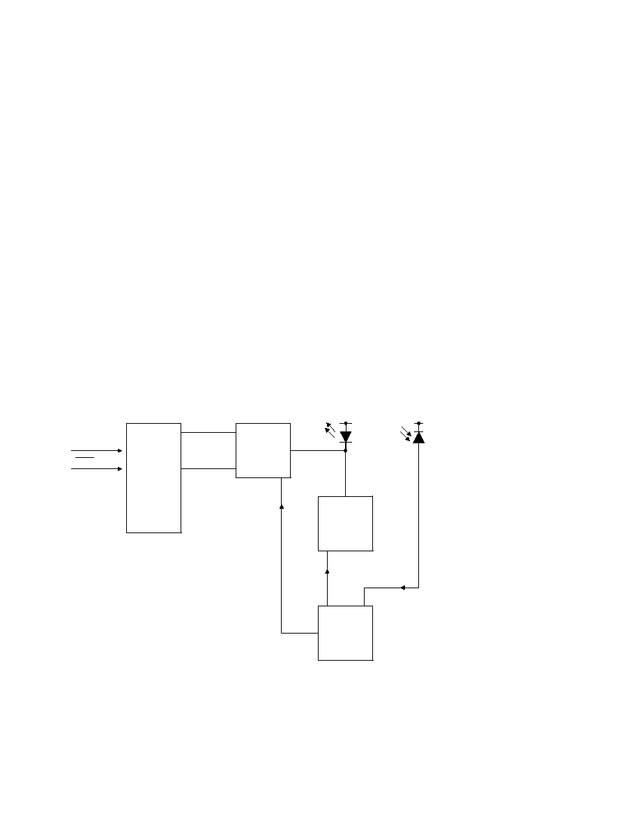
Functional Description
Transmitter Section
Design
The transmitter section, Figure 3,
uses a Multiple Quantum Well
laser as its optical source. The
package of this laser is designed
to allow repeatable coupling into
single mode fiber. In addition, this
package has been designed to be
compliant with IEC 825 Class 1
and CDRH Class I eye safety
requirements. The optical output
is controlled by a custom IC
which detects the laser output via
the monitor photodiode. This IC
provides both dc and ac current
drive to the laser to ensure correct
modulation, eye diagram and
extinction ratio over temperature,
supply voltage and life.
PCB mounting
The HFCT-5205 has two
solderable mounting studs,
Figures 5 and 6. These studs are
not electrically connected. The
transceiver is designed for
common production processes. It
may be wave soldered and
aqueous washed providing the
process plug is in place.
Each process plug can only be
used once during processing,
although with subsequent use, it
can be used as a dust cover.
Figure 3 - Simplified Transmitter Schematic
DATA
DATA
PECL
INPUT
LASER
MODULATOR
LASER
LASER BIAS
DRIVER
LASER BIAS
CONTROL
PHOTODIODE
(rear facet monitor)

5
Figure 4 - Recommended Circuit Schematic
Regulatory Compliance
NO INTERNAL
CONNECTION
NO INTERNAL
CONNECTION
TOP VIEW
V
EER
1
RD
2
SD
4
V
CCR
5
V
CCT
6
TD
8
V
EET
9
NOTES:
THE SPLIT-LOAD TERMINATIONS FOR ECL SIGNALS
NEED TO BE LOCATED AT THE INPUT OF DEVICES
RECEIVING THOSE ECL SIGNALS. RECOMMEND
4-LAYER PRINTED CIRCUIT BOARD WITH 50
W
MICROSTRIP SIGNAL PATHS BE USED.
R1 = R4 = R6 = R8 = R10 = 130
W
R2 = R3 = R5 = R7 = R9 = 82
W
C1 = C2 = 10 µF (see Figure 2)
C3 = C4 = C7 = C8 = 100 nF
C5 = C6 = 0.1 µF
L1 = L2 = 3.3 µH COIL OR FERRITE INDUCTOR.
TERMINATE
AT THE
DEVICE
INPUTS
V
cc
FILTER
AT V
cc
PINS
TRANSCEIVER
V
CC
C8
C1
L1
L2
TD
RD
3
TD
7
R8
RD
RD
V
CC
R5
R7
R6
C6
SD
R10
C7
C2
C3
C4
R4
V
CC
R2
R3
R1
TERMINATION
AT
TRANSCEIVER
INPUTS
TD
C5
R9
Feature
Test Method
Performance
Electrostatic Discharge
(ESD) to the Electrical
Pins
MIL-STD-883C
Method 3015.4
Class 1 (>1 kV) - Human Body Model
Electrostatic Discharge
(ESD) to the Duplex SC
Receptacle
Variation of IEC 801-2
Products of this type, typically, withstand at least 25 kV
without damage when the Duplex SC Connector
Receptacle is contacted by a Human Body Model probe.
Electromagnetic
Interference (EMI)
FCC Class B
CENELEC EN55022 Class B
(CISPR 22A)
VCCI Class 1
Typically provide a 17 dB margin to the noted standard
limits up to 6 GHz, when tested in a GTEM cell with the
transceiver mounted to a circuit card with a chassis
enclosure.
Immunity
Variation of IEC 801-3
Typically show no measurable effect from a 10 V/m field
swept from 27 MHz to 1 GHz applied to the transceiver
without a chassis enclosure.
Eye Safety
FDA CDRH 21-CFR 1040
Class I
CDRH Accession Number: 9521220-26
IEC 825 Issue 1 1993:11
Class 1
CENELEC EN60825 Class 1
TUV Bauart License: 933/510018/02
Document Outline
- Features
- Applications
- Description
- Connection Diagram
- Pin Descriptions
- Functional Description
- Receiver Section
- Design
- Noise Immunity
- Terminating the Outputs
- The Signal Detect Circuit
- Transmitter Section
- Regulatory Compliance
- Performance Specifications
- Absolute Maximum Ratings
- Operating Environment
- Transmitter Section
- Receiver Section
- Ordering Information
- Supporting Documentation
- Handling Precautions