
Agilent HFCT-5942xxx Single Mode Laser
Small Form Factor Transceivers for
ATM, SONET OC-48/SDH STM-16
Part of the Agilent METRAK family
Data Sheet
Description
The HFCT-5942xxx are high
performance, cost effective
modules for serial optical data
communications applications at
2488 Mb/s. They are designed
to provide SONET/SDH
compliant links at 2488 Mb/s
for both short and
intermediate reach links.
The modules are designed for
single mode fiber and operate
at a nominal wavelength of
1300 nm. They incorporate
high performance, reliable, long
wavelength optical devices and
proven circuit technology to
give long life and consistent
service.
The transmitter section of the
HFCT-5942L/AL/G/AG
incorporates a 1300 nm Fabry
Perot (FP) laser. The
transmitter in the HFCT-
5942TL/ATL/TG/ATG uses a
Distributed Feedback (DFB)
Laser packaged in conjunction
with an optical isolator for
excellent back reflection
performance. The transmitter
has full IEC 825 and CDRH
Class 1 eye safety.
For each device the receiver
section uses an MOVPE grown
planar SEDET PIN
photodetector for low dark
current and excellent
responsivity.
A positive ECL logic interface
simplifies interface to external
circuitry.
The transceivers are supplied
in the new industry standard
2 x 10 DIP style package with
the LC fiber connector
interface and is footprint
compatible with SFF Multi
Source Agreement (MSA).
Features
∑ HFCT-5942L/AL:
Links of 2 km with 9/125 µm
single mode fiber (SMF)
∑ HFCT-5942TL/ATL:
Links of 15 km with 9/125 µm
single mode fiber (SMF)
∑ Multisourced 2 x 10 package style
with LC receptacle
∑ Single +3.3 V power supply
∑ Temperature range:
HFCT-5942L/G:
0∞C to +70∞C
HFCT-5942TL/TG:
0∞C to +70∞C
HFCT-5942AL/AG: -40∞C to +85∞C
HFCT-5942ATL/ATG:
-20∞C to +85∞C
∑ Wave solder and aqueous wash
process compatible
∑ Manufactured in an ISO9002
certified facility
∑ Fully Class 1 CDRH/IEC 825
compliant
∑ Compliant with ITU-T G.957
STM-16, I-16 and S-16.1 Optical
Interfaces
∑ HFCT-5942L/AL/TL/ATL:
with EMI nose shield
∑ HFCT-5942G/AG/TG/ATG:
without EMI nose shield
Applications
∑ SONET/SDH equipment
interconnect, OC-48/SDH STM-16
rate
∑ Short and intermediate reach
ATM/SONET links
2
Functional Description
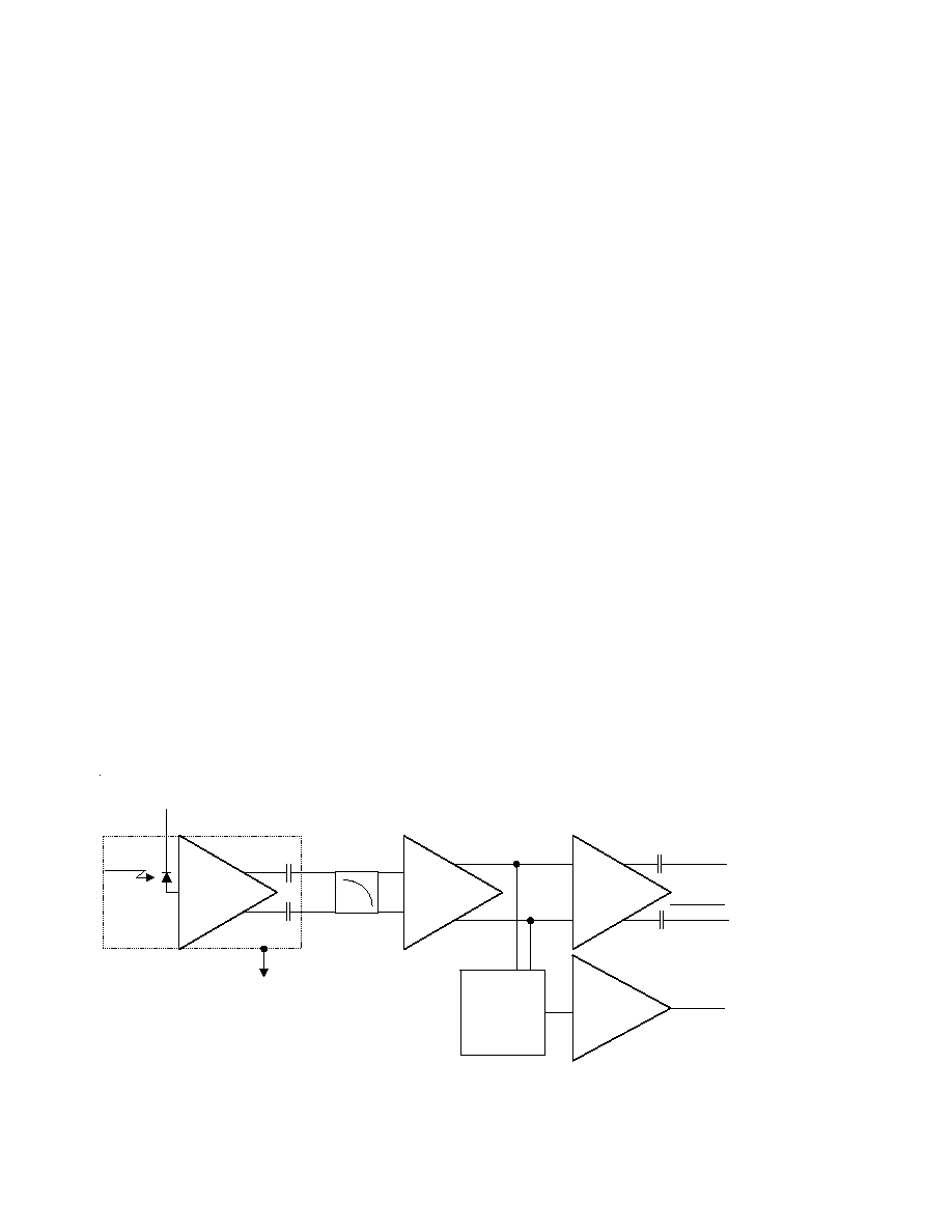
Receiver Section
Design
The receiver section for the
HFCT-5942xxx contains an
InGaAs/InP photo detector and
a preamplifier mounted in an
optical subassembly. This
optical subassembly is coupled
to a postamp/decision circuit
on a circuit board. The design
of the optical assembly is such
that it provides better than 27
dB Optical Return Loss (ORL).
The postamplifier is ac coupled
to the preamplifier as
illustrated in Figure 1. The
coupling capacitors are large
enough to pass the SONET/
SDH test pattern at 2488 Mb/s
without significant distortion
or performance penalty. If a
lower signal rate, or a code
which has significantly more
low frequency content is used,
sensitivity, jitter and pulse
distortion could be degraded.
Figure 1 also shows a filter
function which limits the
bandwidth of the preamp
output signal. The filter is
designed to bandlimit the
preamp output noise and thus
improve the receiver
sensitivity.
These components will reduce
the sensitivity of the receiver
as the signal bit rate is
increased above 2488 Mb/s.
As an optional feature the
device also incorporates a
photodetector bias circuit. The
circuit works by providing a
mirrored output of the bias
current within the photodiode.
This output must be connected
to V
CC
and can be monitored
by connecting through a series
resistor (see Application
Section).
Figure 1. Receiver Block Diagram
Noise Immunity
The receiver includes internal
circuit components to filter
power supply noise. However
under some conditions of EMI
and power supply noise,
external power supply filtering
may be necessary (see
Application Section).
The Signal Detect Circuit
The signal detect circuit works
by sensing the peak level of
the received signal and
comparing this level to a
reference. The SD output is
low voltage TTL.
TRANS-
IMPEDANCE
PRE-
AMPLIFIER
FILTER
GND
AMPLIFIER
PECL
OUTPUT
BUFFER
TTL
OUTPUT
BUFFER
DATA OUT
SIGNAL
DETECT
CIRCUIT
SD
DATA OUT
PHOTODETECTOR
BIAS
3
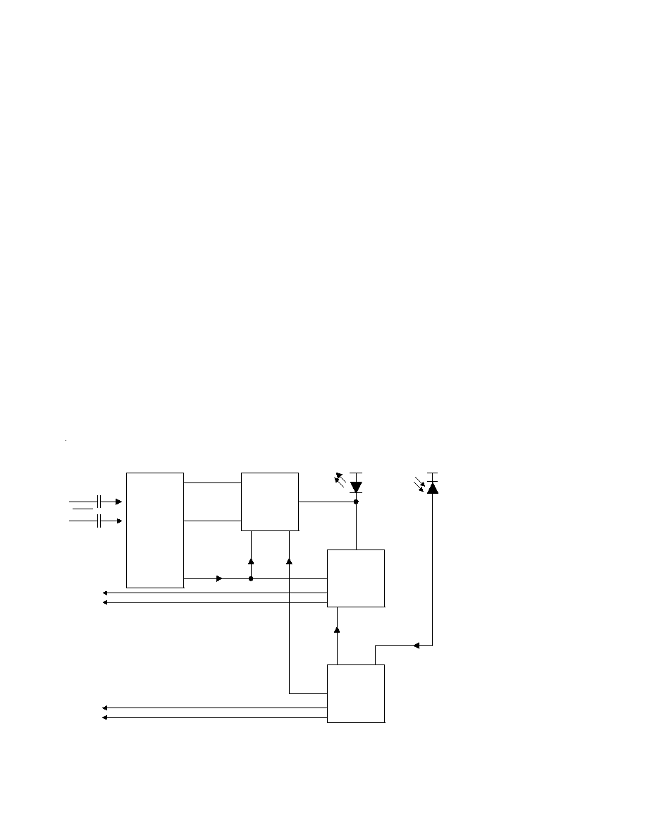
Figure 2. Simplified Transmitter Schematic
Functional Description
Transmitter Section
Design
A schematic diagram for the
transmitter is shown in Figure
2. The HFCT-5942L/AL/G/AG
incorporates an FP laser and
the HFCT-5942TL/TG/ATL/ATG
uses a DFB packaged in
conjunction with an optical
isolator. Both packages have
been designed to be compliant
with IEC 825 eye safety
requirements under any single
fault condition and CDRH
under normal operating
conditions. The optical output
is controlled by a custom IC
that detects the laser output
via the monitor photodiode.
This IC provides both dc and
ac current drive to the laser to
ensure correct modulation, eye
diagram and extinction ratio
over temperature, supply
voltage and operating life.
The transmitters also include
monitor circuitry for both the
laser diode bias current and
laser diode optical power.
DATA
DATA
PECL
INPUT
LASER
MODULATOR
FP or
DFB
LASER
LASER BIAS
DRIVER
LASER BIAS
CONTROL
PHOTODIODE
(rear facet monitor)
B
MON
(+)
B
MON
(-)
P
MON
(+)
P
MON
(-)
4
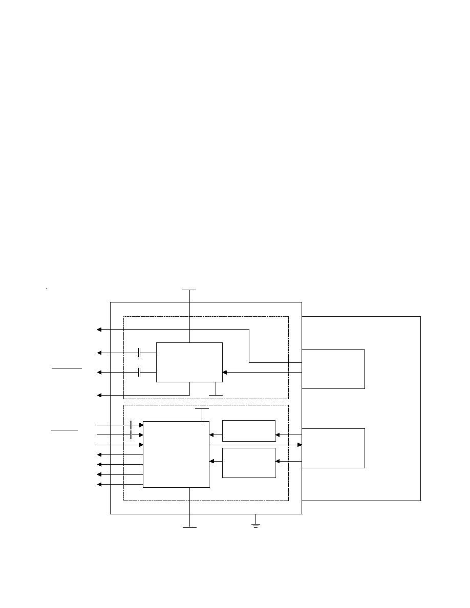
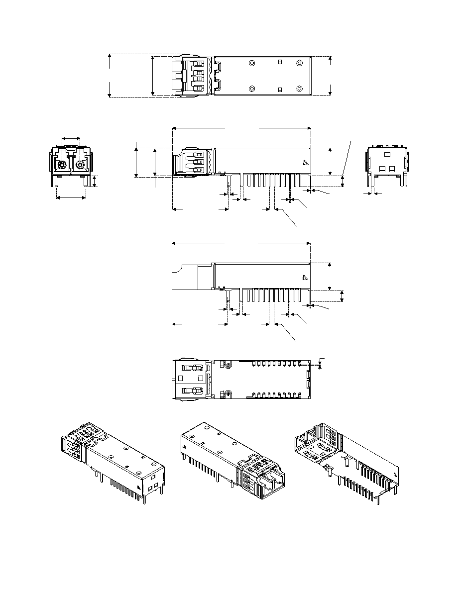
Package
The overall package concept
for the device consists of the
following basic elements; two
optical subassemblies, two
electrical subassemblies and
the housing as illustrated in
the block diagram in Figure 3.
The package outline drawing
and pin out are shown in
Figures 4 and 5. The details of
this package outline and pin
out are compliant with the
multisource definition of the 2
x 10 DIP.
A metallic nose clip provides
connection to chassis ground
for both EMI and thermal
dissipation.
The electrical subassemblies
consist of high volume
multilayer printed circuit
boards on which the IC and
various surface-mounted
passive circuit elements are
attached.
The receiver electrical
subassembly includes an
internal shield for the
electrical and optical
subassembly to ensure high
immunity to external EMI
fields.
The optical subassemblies are
each attached to their
respective transmit or receive
electrical subassemblies. These
two units are then fitted
within the outer housing of the
transceiver that is molded of
filled nonconductive plastic to
provide mechanical strength.
The housing is then encased
with a metal EMI protective
shield. The case is signal
ground and we recommend
soldering the four ground tabs
to host card signal ground.
The pcb's for the two electrical
subassemblies both carry the
signal pins that exit from the
bottom of the transceiver. The
solder posts are fastened into
the molding of the device and
are designed to provide the
mechanical strength required
to withstand the loads
imposed on the transceiver by
mating with the LC
connectored fiber cables.
Although they are not
connected electrically to the
transceiver, it is recommended
to connect them to chassis
ground.
Figure 3. Block Diagram
DATA OUT
SIGNAL
DETECT
DATA IN
DATA IN
Tx DISABLE
B
MON
(+)
B
MON
(-)
P
MON
(+)
P
MON
(-)
QUANTIZER IC
LASER DRIVER
AND CONTROL
CIRCUIT
PIN PHOTODIODE
PREAMPLIFIER
SUBASSEMBLY
LASER
OPTICAL
SUBASSEMBLY
DATA OUT
LC
RECEPTACLE
R
X
SUPPLY
T
X
SUPPLY
R
X
GROUND
T
X
GROUND
PHOTO DETECTOR
BIAS
LASER BIAS
MONITORING
LASER DIODE
OUTPUT POWER
MONITORING
CASE
*
* NOSE CLIP PROVIDES CONNECTION TO CHASSIS GROUND FOR BOTH EMI AND THERMAL DISSIPATION.
5
Figure 4. HFCT-5942xxx Package Outline Drawing
BOTTOM VIEW
NOTE: END OF PINS
CHAMFERED
TOP VIEW
13.59
(0.535)
MAX
13.59
0.535
+ 0
- 0.2
+0
-0.008
( )
15.0 ± 0.2
(0.591 ± 0.008)
6.25
(0.246)
9.8
(0.386)
MAX
FRONT VIEW
SIDE VIEW
BACK VIEW
19.5 ±0.3
(0.768 ±0.012)
DIMENSIONS IN MILLIMETERS (INCHES)
DIMENSIONS SHOWN ARE NOMINAL. ALL DIMENSIONS MEET THE MAXIMUM PACKAGE OUTLINE DRAWING IN THE SFF MSA.
9.8
(0.386)
MAX
SIDE VIEW
19.5 ±0.3
(0.768 ±0.012)
G MODULE - NO EMI NOSE SHIELD
48.5 ± 0.2
(1.91 ± 0.008)
ÿ 1.07 ± 0.1
(0.042 ± 0.004)
1 ± 0.1
(0.039 ± 0.004)
1 ± 0.1
(0.039 ± 0.004)
4.06 ± 0.1
(0.16 ± 0.004)
20 x 0.5 ± 0.2
(0.02 ± 0.008)
0.25 ± 0.1
(0.01 ± 0.004)
1.78 ± 0.1
(0.07 ± 0.004)
10.16 ± 0.1
(0.4 ± 0.004)
3.81 ± 0.15
(0.15 ± 0.006)
9.6 ± 0.2
(0.378 ±0.008)
10.8 ± 0.2
(0.425 ± 0.008)
ÿ 1.07 ± 0.1
(0.042 ± 0.004)
1 ± 0.1
(0.039 ± 0.004)
1.78 ± 0.1
(0.07 ± 0.004)
20 x 0.5 ± 0.2
(0.02 ± 0.008)
0.25 ± 0.1
(0.01 ± 0.004)
3.81 ± 0.1
(0.15 ± 0.004)
20 x 0.25 ± 0.1 (PIN THICKNESS)
(0.01 ± 0.004)
48.5 ± 0.2
(1.91 ± 0.008)