1-161
H
Subminiature High Performance
AlInGaP LED Lamps
Technical Data
Features
· Subminiature Flat Top
Package
Ideal for Backlighting and Light
Piping Applications
· Subminiature Dome Package
Nondiffused Dome for High
Brightness
· Wide Range of Drive
Currents
· Colors: 590 nm Amber,
615 nm Reddish-Orange
· Ideal for Space Limited
Applications
· Axial Leads
· Available with Lead
Configurations for Surface
Mount and Through Hole PC
Board Mounting
Description
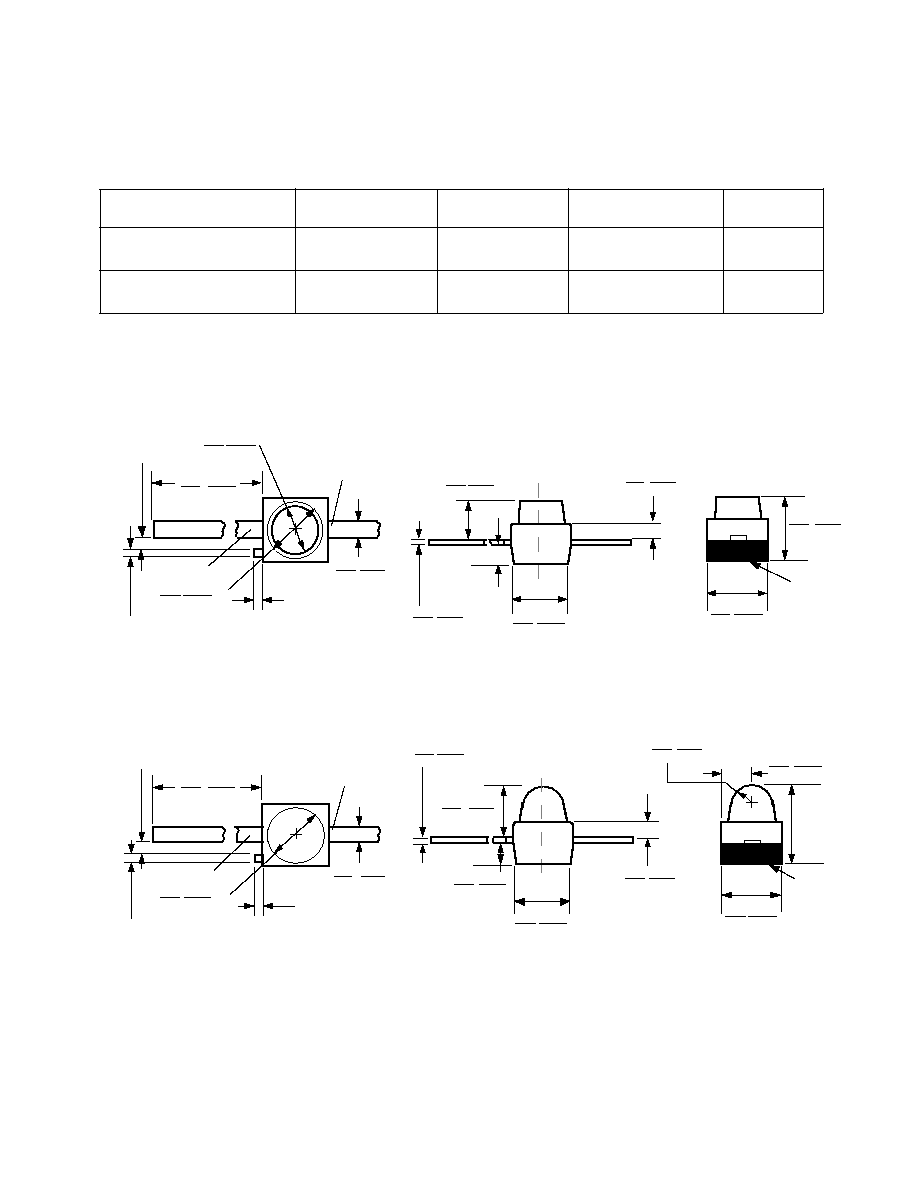
Flat Top Package
The HLMX-PXXX flat top lamps
use an untinted, nondiffused,
truncated lens to provide a wide
radiation pattern that is necessary
for use in backlighting applica-
tions. The flat top lamps are also
ideal for use as emitters in light
pipe applications.
Dome Packages
The HLMX-QXXX dome lamps use
an untinted, nondiffused lens to
provide a high luminous intensity
within a narrow radiation pattern.
Lead Configurations
All of these devices are made by
encapsulating LED chips on axial
lead frames to form molded epoxy
subminiature lamp packages. A
variety of package configuration
options is available. These include
special surface mount lead
configurations, gull wing, yoke
lead, or Z-bend. Right angle lead
bends at 2.54 mm (0.100 inch)
and 5.08 mm (0.200 inch) center
spacing are available for through
hole mounting. For more infor-
mation refer to Standard SMT and
Through Hole Lead Bend Options
for Subminiature LED Lamps data
sheet.
Technology
These subminiature solid state
lamps utilize one of the two newly
developed aluminum indium
gallium phosphide (AlInGaP) LED
technologies, either the absorbing
substrate carrier technology (AS
= HLMA-Devices) or the
transparent substrate carrier
technology (TS = HLMT-
Devices). The TS HLMT-Devices
are especially effective in very
bright ambient lighting condi-
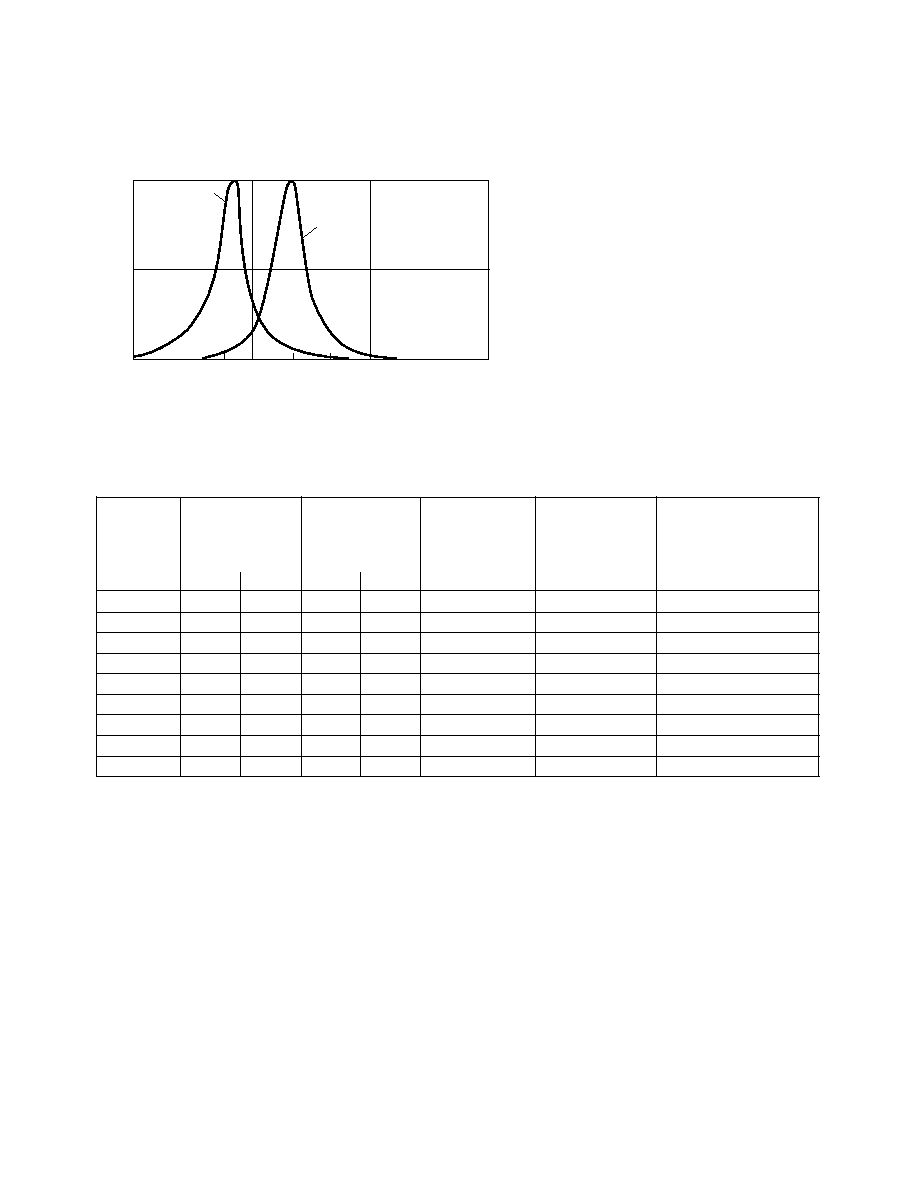
tions. The colors 590 nm amber
and 615 nm reddish-orange are
available with viewing angles of
15
°
for the domed devices and
125
°
for the flat top devices.
SunPower Series
HLMA-PH00
HLMT-PH00
HLMA-PL00
HLMT-PL00
HLMA-QH00 HLMT-QH00
HLMA-QL00
HLMT-QL00
5964-9364E

1-163
Absolute Maximum Ratings at T
A
= 25
°
C
HLMA-QL00/QH00/PL00/PH00
Peak Forward Current
[2]
........................................................... 200 mA
Average Forward Current (I
PEAK
= 200 mA)
[1,2]
......................... 45 mA
DC Forward Current
[3,5,6]
........................................................... 50 mA
Power Dissipation .................................................................... 105 mW
HLMT-QL00/QH00/PL00/PH00
Peak Forward Current
[2]
........................................................... 100 mA
Average Forward Current (I
PEAK
= 100 mA)
[1,2]
......................... 37 mA
DC Forward Current
[3,5,6]
........................................................... 50 mA
Power Dissipation .................................................................... 120 mW
All Devices
Reverse Voltage (I
R
= 100
µ
A) ........................................................ 5 V
Transient Forward Current (10
µ
s Pulse)
[5]
.............................. 500 mA
Operating Temperature Range ....................................... -40 to +100
°
C
Storage Temperature Range .......................................... -55 to +100
°
C
LED Junction Temperature .......................................................... 110
°
C
Lead Soldering Temperature
[1.6 mm (0.063 in.) from body .......................... 260
°
C for 5 seconds
SMT Reflow Soldering Temperatures
Convective Reflow ............. 235
°
C Peak, above 183
°
C for 90 seconds
Vapor Phase Reflow ........................................... 215
°
C for 3 minutes
Notes:
1. Maximum I
AVG
at f = 1 kHz.
2. Refer to Figure 6 to establish pulsed operating conditions.
3. Derate linearly as shown in Figure 4.
4. The transient peak current is the maximum non-recurring peak current these devices
can withstand without damaging the LED die and wire bonds. Operation at currents
above Absolute Maximum Peak Forward Current is not recommended.
5. Drive currents between 5 mA and 30 mA are recommended for best long term
performance.
6. Operation at currents below 5 mA is not recommended, please contact your Hewlett-
Packard sales representative.
1-164
Optical Characteristics at T
A
= 25
°
C
Luminous
Color,
Viewing
Intensity
Total Flux
Peak
Dominant
Angle
Luminous
Part
I
V
(mcd)
V
(mlm)
Wavelength
Wavelength
2
1/2
Efficacy
Number
@ 20 mA
[1]
@ 20 mA
[2]
peak
(nm)
d
[3]
(nm)
Degrees
[4]
v
[5]
HLMA-
Min. Typ.
Typ.
Typ.
Typ.
Typ.
(lm/w)
QL00
135
500
250
592
590
15
480
QH00
135
500
250
621
615
15
263
PL00
23
75
250
592
590
125
480
PH00
22
75
250
621
615
125
263
HLMT-
QL00
300 800
592
590
15
480
QH00
290
800
800
621
615
15
263
PL00
46
150
800
592
590
125
480
PH00
35
120
800
621
615
125
263
Notes:
1. The luminous intensity, I
v
, is measured at the mechanical axis of the lamp package. The actual peak of the spatial radiation pattern
may not be aligned with this axis.
2.
v
is the total luminous flux output as measured with an integrating sphere.
3. The dominant wavelength,
d
, is derived from the CIE Chromaticity Diagram and represents the color of the device.
4.
1/2
is the off-axis angle where the liminous intensity is 1/2 the peak intensity.
5. Radiant intensity, I
v
, in watts/steradian, may be calculated from the equation I
v
= I
v
/
v
, where I
v
is the luminous intensity in candelas
and
v
is the luminous efficacy in lumens/watt.
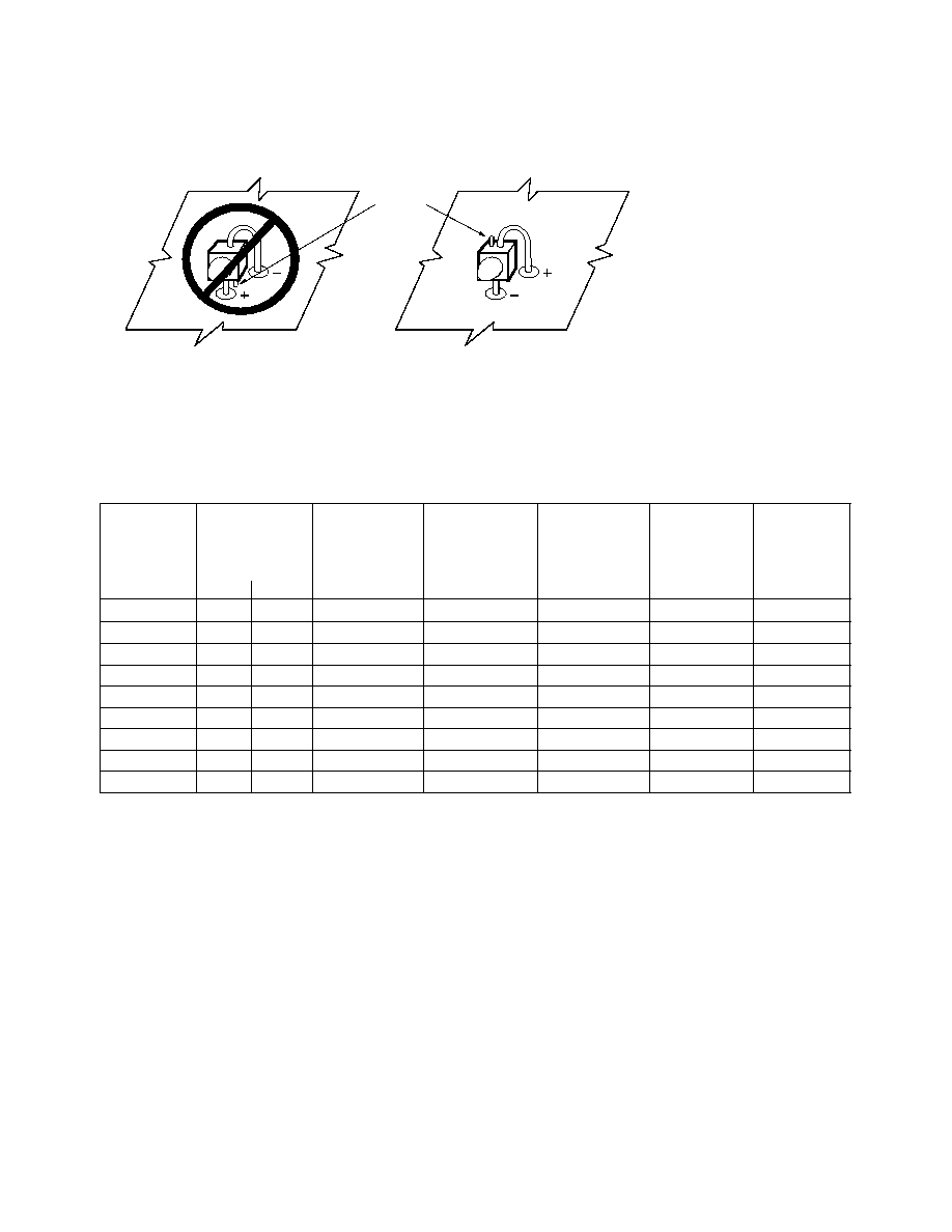
NO. ANODE DOWN.
YES. CATHODE DOWN.
CATHODE
TAB
Figure 1. Proper Right Angle Mounting to a PC Board to Prevent Protruding Cathode Tab from Shorting to Anode
Connection.
1000