HLMP-7000, -7019, -7040
T-1
3
/
4
(5 mm), T-1 (3 mm), Low
Current LED Lamps
Technical Data
Features
∑ Low Power
∑ High Efficiency
∑ CMOS-MOS Compatible
∑ TTL Compatible
∑ Wide Viewing Angle
∑ Choice of Package Styles
∑ Choice of Colors
Applications
∑ Low Power DC Circuits
∑ Telecommunications
Indicators
∑ Portable Equipment
∑ Keyboard Indicators
Description
These tinted diffused LED lamps
are designed and optimized
specifically for low DC current
operation. Luminous intensity and
forward voltage are tested at
2 mA to assure consistent bright-
ness at TTL output current levels.
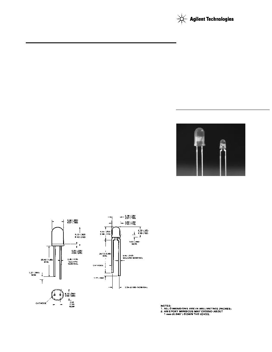
Package Dimensions
HLMP-4700, -4719, -4740
HLMP-1700, -1719, -1790
A
B
HLMP-1700, -1719, -1790
HLMP-4700, -4719, -4740
2
Note:
1.
1
/
2
is the typical off-axis angle at which the luminous intensity is half the axial luminous intensity.
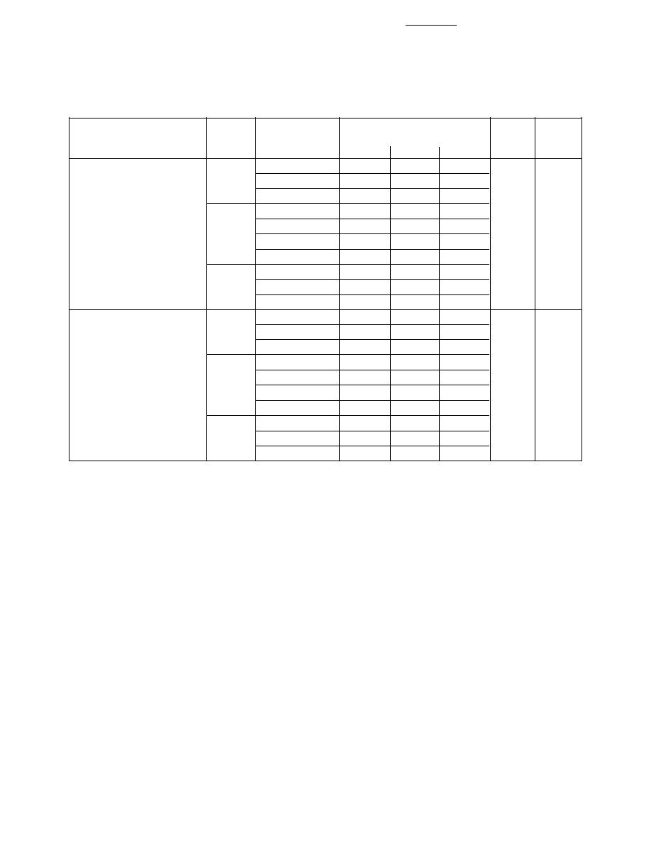
Selection Guide
Luminous Intensity Iv (mcd)
at 2 mA
Package
Package Description
Color
Device HLMP-
Min.
Typ.
Max.
2
1/2
Outline
T-1 3/4 Tinted Diffused
Red
4700
1.5
2.3
≠
50
A
4700-C00xx
1.5
2.3
≠
4700-CD0xx
1.3
2.3
4.2
Yellow
4719
0.9
2.1
≠
4719-A00xx
0.9
2.1
≠
4719-BC0xx
1.4
2.5
4.4
4719-BCBxx
1.4
2.5
4.4
Green
4740
1.0
2.3
≠
4740-A00xx
1.0
2.3
≠
4740-AB0xx
1.0
2.3
3.2
T-1 Tinted Diffused
Red
1700
0.8
2.1
≠
50
B
1700-B0000
0.8
2.1
≠
1700-CD000
1.3
2.3
4.2
Yellow
1719
0.9
2.1
≠
1719-A0000
0.9
2.1
≠
1719-AB000
0.9
2.1
2.8
1719-ABB00
0.9
2.1
2.8
Green
1790
1.0
2.3
≠
1790-A0000
1.0
2.3
≠
1790-AB000
1.0
2.4
3.2
3
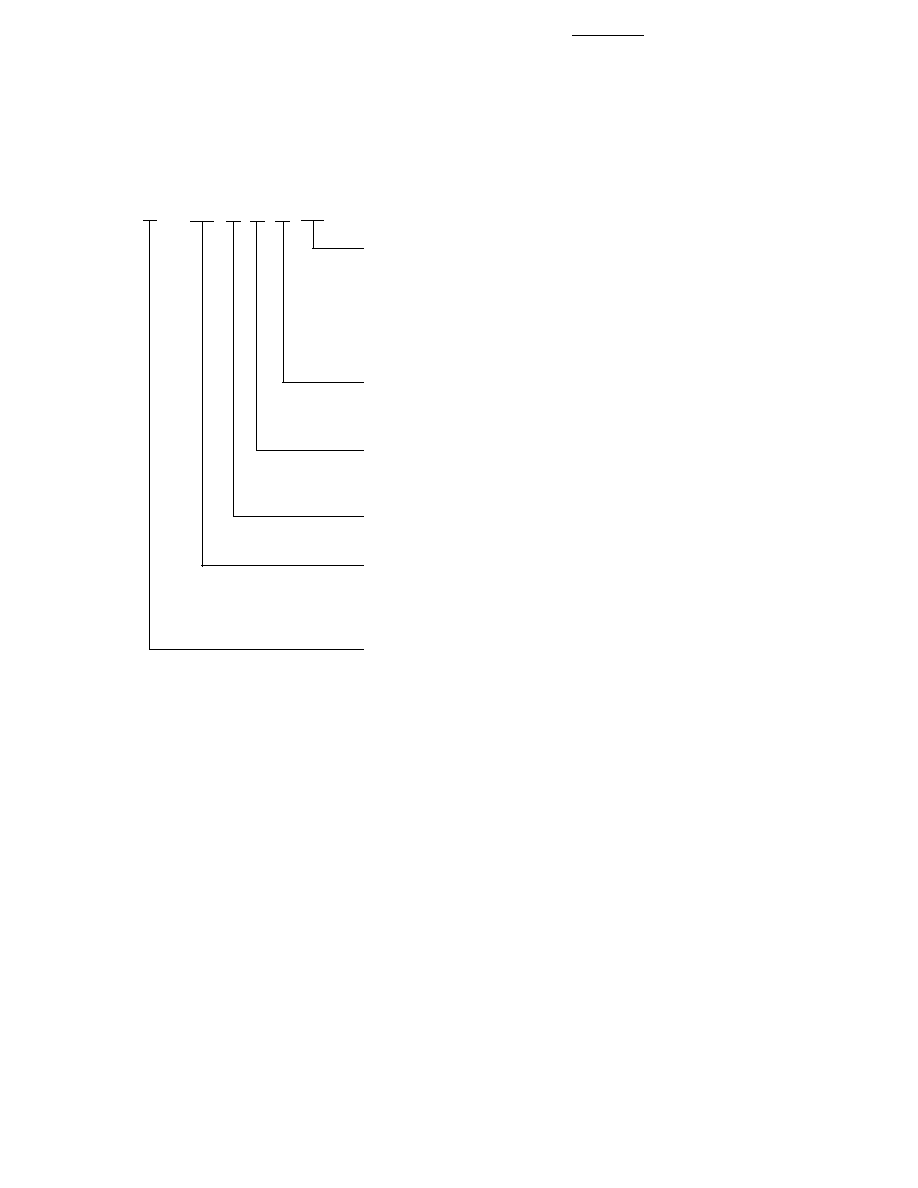
Part Numbering System
HLMP-X
7
XX
X
X
X
XX
Mechanical Option
00: Bulk
01: Tape & Reel, Crimped Leads
02, BH: Tape & Reel, Straight Leads
A1, B1: Right Angle Housing, Uneven Leads
A2, B2: Right Angle Housing, Even Leads
R1: Tape & Reel, Crimped Leads, Counter Clockwise
Color Bin Options
0: Full color bin distribution
B: Color bins 2 & 3 only
Maximum Iv Bin Options
0: Open (No. max. limit)
Others: Please refer to the Iv bin Table
Minimum Iv Bin Options
Please refer to the Iv Bin Table
Color Option
00: GaP HER
19: GaP Yellow
40: GaP Green
Package Options
4: T-1
3
/
4
(5 mm)
1: T-1 (3 mm)
4
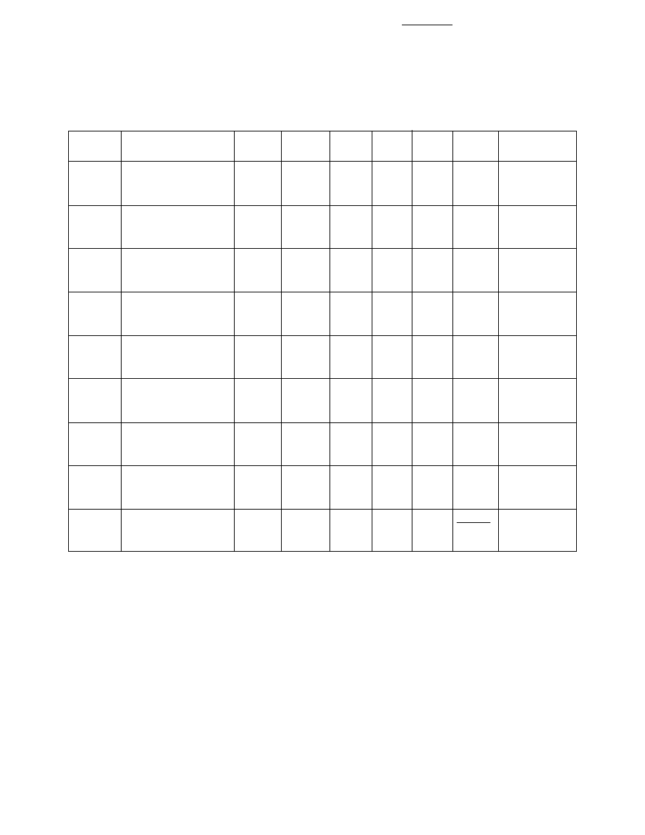
Electrical/Optical Characteristics at T
A
= 25
∞
C
Test
Symbol
Description
T-1
3
/
4
T-1
Min.
Typ.
Max.
Units
Conditions
V
F
Forward Voltage
4700
1700
1.7
2.0
V
2 mA
4719
1719
1.8
2.5
4740
1790
1.9
2.2
V
R
Reverse Breakdown
4700
1700
5.0
V
I
R
= 50
µ
A
Voltage
4719
1719
5.0
4740
1790
5.0
d
Dominant
4700
1700
626
nm
Note 1
Wavelength
4719
1719
585
4740
1790
569
1/2
Spectral Line
4700
1700
40
nm
Halfwidth
4719
1719
36
4740
1790
28
S
Speed of Response
4700
1700
90
ns
4719
1719
90
4740
1790
500
C
Capacitance
4700
1700
11
pF
V
F
= 0,
4719
1719
15
f = 1 MHz
4740
1790
18
R
J-PIN
Thermal
4700
1700
260
[3]
∞
C/W
Junction to
Resistance
4719
1719
290
[4]
Cathode Lead
4740
1790
PEAK
Peak Wavelength
4700
1700
635
nm
Measurement
4719
1719
583
at peak
4740
1790
565
V
Luminous Efficacy
4700
1700
145
lumens
Note 2
4719
1719
500
watt
4740
1790
595
Notes:
1. The dominant wavelength,
d
, is derived from the CIE chromaticity diagram and represents the single wavelength which defines the
color of the device.
2. The radiant intensity, I
e
, in watts per steradian, may be found from the equation I
e
= I
V
/
V
, where I
V
is the luminous intensity in
candelas and
V
is luminous efficacy in lumens/watt.
3. T-1
3
/
4
.
4. T-1.
5
Absolute Maximum Ratings
Parameter
Maximum Rating
Units
Power Dissipation
Red
24
mW
(Derate linearly from 92
∞
C at 1.0 mA/
∞
C)
Yellow
36
Green
24
DC and Peak Forward Current
7
mA
Transient Forward Current (10
µ
s Pulse)
[1]
500
mA
Reverse Voltage (I
R
= 50
µ
A)
5.0
V
Operating Temperature Range
Red/Yellow
-55
∞
C to 100
∞
C
Green
-20
∞
C to 100
∞
C
Storage Temperature Range
-55
∞
C to +100
∞
C
Lead Soldering Temperature
260
∞
C for 5 seconds
[1.6 mm (0.063 in.) from body]
Note:
1. The transient peak current is the maximum non-recurring peak current the devices can withstand without damaging the LED die and
wire bonds. It is not recommended that the device be operated at peak currents beyond the Absolute Maximum Peak Forward Current.
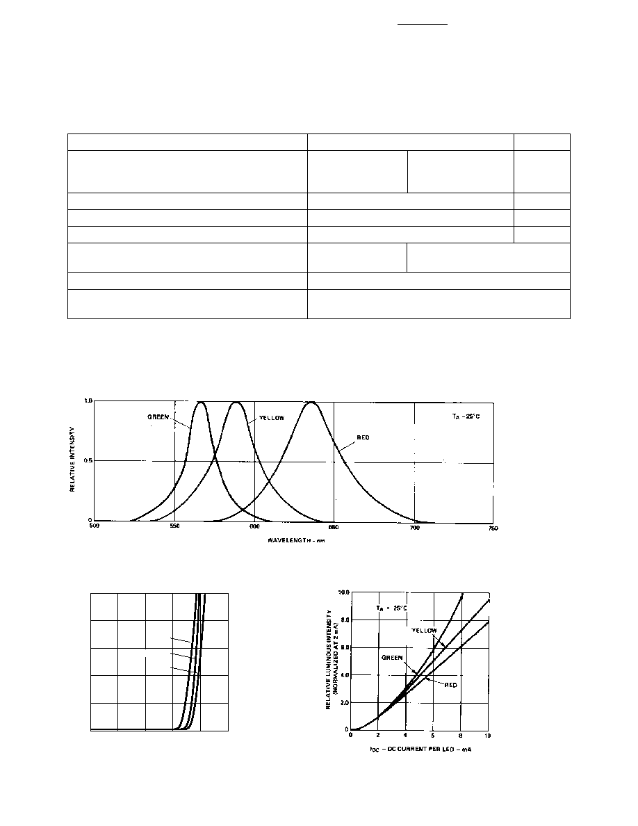
Figure 2. Forward Current vs. Forward Voltage.
Figure 3. Relative Luminous Intensity vs. Forward Current.
Figure 1. Relative Intensity vs. Wavelength.
DC CURRENT ≠ mA
0
0
VOLTAGE ≠ V
1.5
6
0.5
1.0
2.5
2
4
8
10
2.0
RED
YELLOW
GREEN