Description
These Super Bright Precision
Optical Performance LED lamps
are based on flip chip InGaN
material, which is the brightest
and most efficient technology
for LEDs. A blue LED die is
coated with phosphor to
produce white.
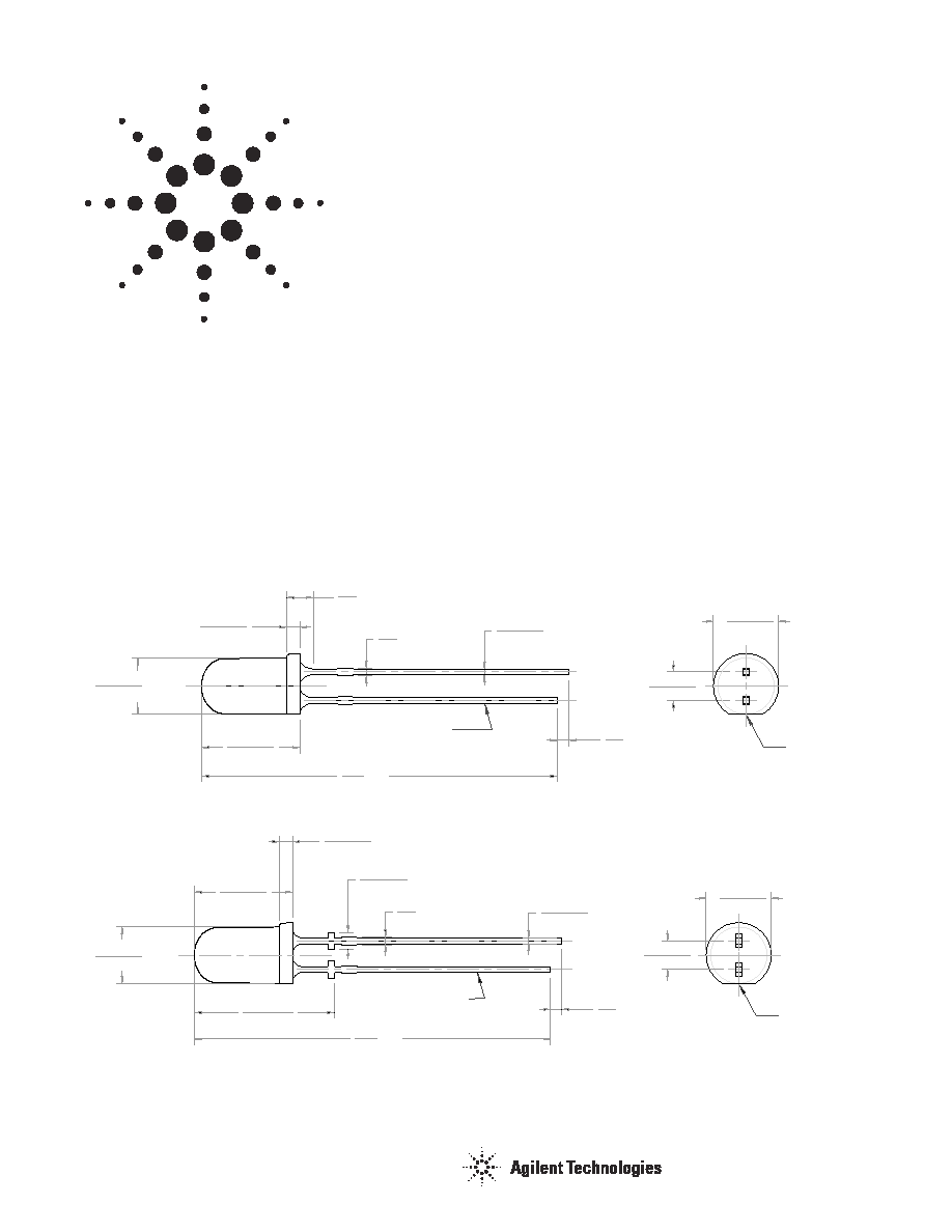
Package Dimension A
Package Dimension B
Dimension H:
23 & 30 Degree = 12.67 +/- 0.25 mm (0.499 +/- 0.01 inch)
15 Degree = 12.93 +/- 0.25 mm (0.509 +/- 0.01 inch)
Notes :
1. Measured just above flange.
2. All dimensions are in milimetres /inches.
3. Epoxy meniscus may extend about 1mm (0.040") down the leads.
.028
0.70 max
.100±.015
2.54±0.38
1.244
31.60 min
.093
2.35 max
.228±.008
¯5.80±0.20
.343±.008
8.71±0.20
.197±.008
5.00±0.20 note#1
.039
1.00 min
.020±.004
0.50±0.10 sq. typ.
.045±.008
1.14±0.20
cathode
flat
cathode
lead
cathode
lead
cathode
flat
.059±.006
1.50±0.15
Dimension H
.343±.008
8.71±0.20
.100±.015
2.54±0.38
1.244
31.60 min
.020±.004
0.50±0.10 sq. typ.
.039
1.00 min
.197±.008
5.00±0.20
.228±.008
¯
5.80±0.20
.028
0.70 max
.045±.008
1.14±0.20
note#1
Refer to Table below.
Agilent HLMP-CW18, HLMP-CW19,
HLMP-CW28, HLMP-CW29,
HLMP-CW38, HLMP-CW39.
T-1 3/4 Precision Optical
Performance White LED
Data Sheet
These T- 1 3/4 lamps
incorporate precise optics which
produce well- defined spatial
radiation patterns at specific
viewing cone angle.
Benefit
∑ Reduced Power Consumption,
Higher Reliability, and Increased
Optical/Mechanical Design
Flexibility Compared to
Incandescent Bulbs and Other
Alternative White Light Sources
Features
∑ Highly Luminous White Emission
∑ 15
o
, 23
o
, and 30
o
viewing angle
∑ New InGaN flip chip die technology
with protective diode.
∑ ESD class 3
Applications
∑ Electronic Signs and Signals
∑ Small Area Illumination
∑ Legend Backlighting
∑ General Purpose Indicators
2
Device Selection Guide
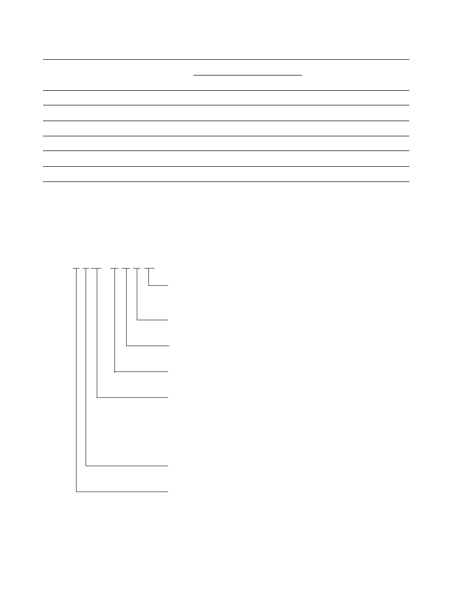
Part Numbering System
Part Number
Typ. Viewing Angle
Iv (cd) @ 20mA
Standoff Leads
Package
Dimension
Min.
Typ.
HLMP-CW18-VY0xx
15
∞
4.20
6.40
No
A
HLMP-CW19-VY0xx
15
∞
4.20
6.40
Yes
B
HLMP-CW28-TW0xx
23
∞
2.50
3.80
No
A
HLMP-CW29-TW0xx
23
∞
2.50
3.80
Yes
B
HLMP-CW38-SV0xx
30
∞
1.90
3.00
No
A
HLMP-CW39-SV0xx
30
∞
1.90
3.00
Yes
B
Notes:
1. Tolerance for luminous intensity measurement is +/- 15%
2. The luminous intensity is measured on the mechanical axis of the lamp package.
3. The optical axis is closely aligned with the package mechanical axis.
4. LED light output is bright enough to cause injuries to the eyes. Precautions must be taken to prevent looking directly at the LED without proper safety
equipment.
Mechanical Option
00: Bulk
DD: Ammo Pack
L M P
Color Bin Options
0: Full color bin distribution
Maximum Intensity Bin Limit
0: No maximum intensity bin limit
Viewing Angle
18: 15 without standoffs
19: 15∞ with standoffs
28: 23∞ without standoffs
29: 23∞ with standoffs
38: 30 ∞ without standoffs
39: 30 ∞ with standoffs
Color Options
W: White
Package Options
C: T-1 3/4
-
-
XX
X
X X XX
C W
Minimum Intensity Bin Limit
Refer to Device Selection Guide

3
Absolute Maximum Ratings (T
A
= 25
∞
C)
Electrical/Optical Characteristics (T
A
= 25
o
C)
Parameter
Value
Units
DC Forward Current
[1]
30
mA
Peak Forward Current
[2]
100
mA
Average Forward Current
30
mA
Power Dissipation
120
mW
LED Junction Temperature
130
∞
C
Operating Temperature Range
-40 to +85
∞
C
Storage Temperature Range
-40 to +100
∞
C
Wave Solder Temperature
[3]
250 for 3 secs
∞
C
Solder Dipping Temperature
[3]
260 for 5secs
∞
C
Notes:
1. Derate linearly as shown in Figure 4.
2. Duty Factor 30%, 1 KHz
3. 1.59 mm (0.060 inch) below body
Parameters
Symbol
Minimum Typical
Maximum Units
Test Condition
Forward voltage
V
F
3.4
4.0
V
I
F
= 20 mA
Capacitance
C
53
pF
V
F
=0, f=1 MHz
Reverse Voltage
[1]
V
R
0.6
V
I
R
= 10
µ
A
Thermal resistance
R
J-PIN
240
o
C/W
LED Junction to cathode lead
Viewing Angle
[2]
CW18/CW19
CW28/CW29
CW38/CW39
2
1/2
15
23
30
Degree
I
F
= 20 mA
Chromaticity Coordinate
[3]
X
Y
0.31
0.32
I
F
= 20 mA
Notes:
1. The reverse voltage of the product is equivalent to the forward voltage of the protective chip at I
R
= 10
µ
A
2. 2
1/2
is the off-axis angle where the luminous intensity is Ω the
on axis intensity
3. The chromaticity coordinates are derived from the CIE 1931 Chromaticity Diagram and represent the perceived color of the device.

4
Figure 1. Relative Intensity vs Wavelength
Figure 2. Forward Current vs Forward Voltage
Figure 3. Relative Iv vs. Forward Current
Figure 4. Maximum Fwd Current vs Temperature
Figure 5. Chromaticity shift vs. current
0.0
0.2
0.4
0.6
0.8
1.0
380
480
580
680
780
Wavelength (nm)
Relative Intensity
0
10
20
30
0
1
2
3
4
Forward Voltage (V)
Forward Current (mA)
0.0
0.3
0.6
0.9
1.2
1.5
0
10
20
30
DC Forward Current (mA)
Relative Luminous Intensity
0
5
10
15
20
25
30
35
0
20
40
60
80
100
Ambient Temperature (C)
Maximum Forward Current (mA)
R
J-A
= 780∞ C/W
R
J-A
= 585∞ C/W
-0.010
-0.005
0
0.005
0.010
0.015
0.020
-0.004
-0.002
0
0.002
0.004
X-Coordinate
Y-Coordinate
30mA
25mA
20mA
15mA
10mA
5mA
1mA
(X,Y) VALUES @ 20mA REFERENCE TO (0,0)
5
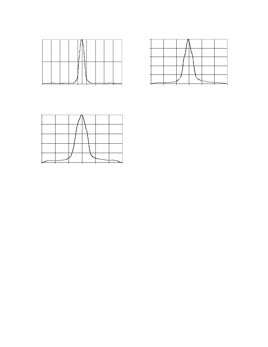
Figure 6a. CW1x Spatial Radiation Pattern
Figure 6b. CW2x Spatial Radiation Pattern
Figure 6c. CW3x Spatial Radiation Pattern
0.0
0.5
1.0
-90
-70
-50
-30
-10
10
30
50
70
90
Angular Displacement (Degree)
Relative Intensity
0.0
0.2
0.4
0.6
0.8
1.0
-90
-60
-30
0
30
60
90
Angular Displacement
Relative Luminous Intensity
0.0
0.2
0.4
0.6
0.8
1.0
-90
-60
-30
0
30
60
90
Angular Displacement
Relative Luminous Intensity