T-1
3
/
4
(5 mm),
T-1 (3 mm), Low
Current, Double Heterojunction
AlGaAs Red LED Lamps
Technical Data
Features
∑ Minimum Luminous Inten-
sity Specified at 1 mA
∑ High Light Output at Low
Currents
∑ Wide Viewing Angle
∑ Outstanding Material
Efficiency
∑ Low Power/Low Forward
Voltage
∑ CMOS/MOS Compatible
∑ TTL Compatible
∑ Deep Red Color
Applications
∑ Low Power Circuits
∑ Battery Powered Equipment
∑ Telecommunication
Indicators
Description
These solid state LED lamps
utilize newly developed double
heterojunction (DH) AlGaAs/GaAs
material technology. This LED
material has outstanding light
output efficiency at very low drive
currents. The color is deep red at
the dominant wavelength of 637
nanometres. These lamps are
ideally suited for use in
applications where high light
output is required with minimum
power output.
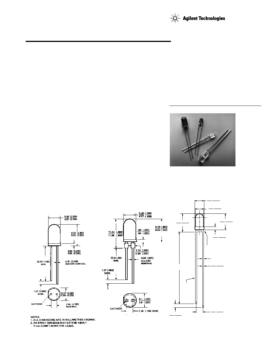
Package Dimensions
B
C
A
HLMP-D150/D155
HLMP-K150/K155
1.14 (0.045)
0.51 (0.020)
3.43 (0.135)
2.92 (0.115)
24.1
(0.95)
MIN.
4.70 (0.185)
4.19 (0.165)
3.17 (0.125)
2.67 (0.105)
2.79 (0.110)
2.29 (0.090)
1.52 (0.060)
1.02 (0.040)
6.35 (0.250)
5.58 (0.220)
0.55 (0.022)
0.40 (0.016)
CATHODE
0.65 (0.026) MAX.
SQ. TYP.
SHOULDER
2
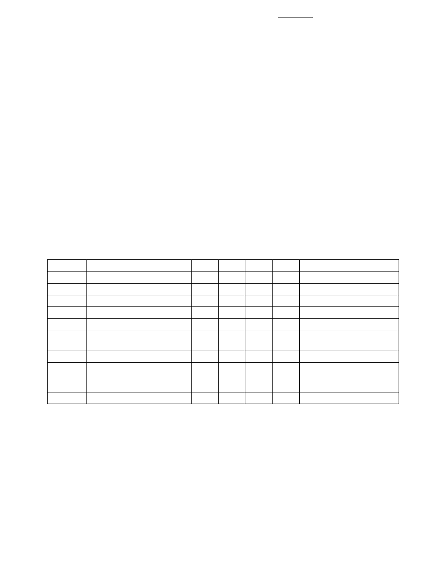
Selection Guide
Luminous Intensity Iv (mcd)
at 1 mA
2
1/2[1]
Package
Package Description
Device HLMP-
Min.
Typ.
Max.
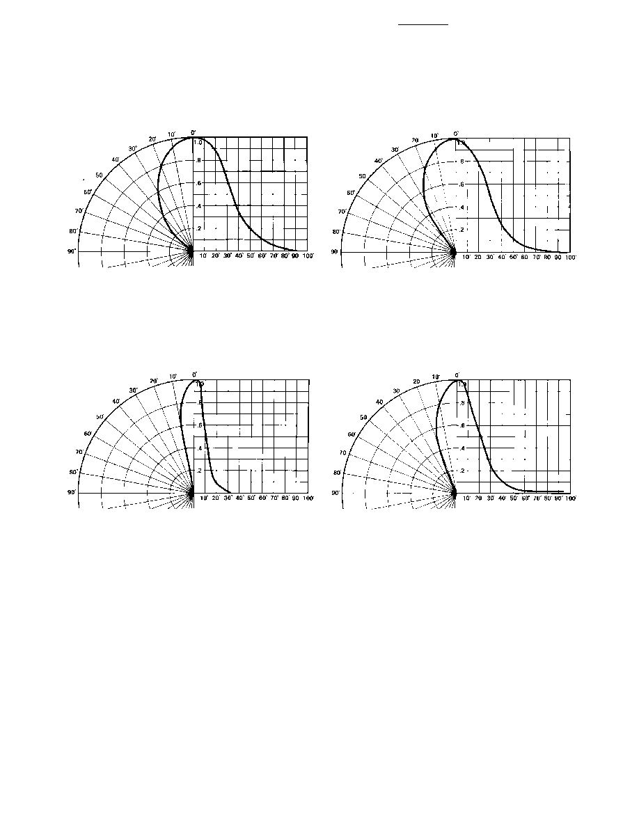
Degree
Outline
T-1 3/4 Red Tinted Diffused
D150
1.3
3.0
≠
65
A
D150-C00xx
1.3
3.0
≠
65
A
D150-CD0xx
1.3
3.0
4.2
65
A
T-1 3/4 Red Untinted Non-diffused
D155
5.4
10.0
≠
24
B
D155-F00xx
5.4
10.0
≠
24
B
T-1 Red Tinted Diffused
K150
1.3
2.0
≠
60
C
K150-C00xx
1.3
2.0
≠
60
C
K150-CD0xx
1.3
3.0
4.2
60
C
T-1 Red Untinted Non-diffused
K155
2.1
3.0
≠
45
C
K155-CD0xx
1.3
3.0
4.2
45
C
K155-D00xx
2.1
3.0
≠
45
C
K155-DE0xx
2.1
3.0
6.8
45
C
Part Numbering System
Note:
1.
1/2
is the off axis angle from lamp centerline where the luminous intensity is
1
/
2
the on-axis value.
HLMP - x 1 xx - x x x xx
Mechanical Option
00: Bulk
01: Tape & Reel, Crimped Leads
02: Tape & Reel, Straight Leads
A1, B1: Right Angle Housing, Uneven Leads
A2, B2: Right Angle Housing, Even Leads
DD, DH: Ammo Pack
Color Bin Optioms
0: Full color bin distribution
Maximum Iv Bin Options
0: Open (No max. limit)
Others: Please refer to the Iv bin table
Minimum Iv Bin Options
Please refer to the Iv bin table
Lens Option
50: Tinted, Diffused
55: Untinted, Nondiffused
Package Options
D: T-1
3
/
4
(5 mm)
K: T-1 (3 mm)
3
Absolute Maximum Ratings at T
A
= 25
∞
C
Peak Forward Current
[1]
...................................................................................................................... 300 mA
Average Forward Current ....................................................................................................................... 20 mA
DC Current
[2]
......................................................................................................................................... 30 mA
Power Dissipation ................................................................................................................................. 87 mW
Reverse Voltage (I
R
= 100
µ
A).................................................................................................................... 5 V
Transient Forward Current (10
µ
s Pulse)
[3]
......................................................................................... 500 mA
LED Junction Temperature ..................................................................................................................... 110
∞
C
Operating Temperature Range ................................................................................................... -20 to +100
∞
C
Storage Temperature Range ....................................................................................................... -55 to +100
∞
C
Lead Soldering Temperature [1.6 mm (0.063 in.) from body] ........................................... 260
∞
C for 5 seconds
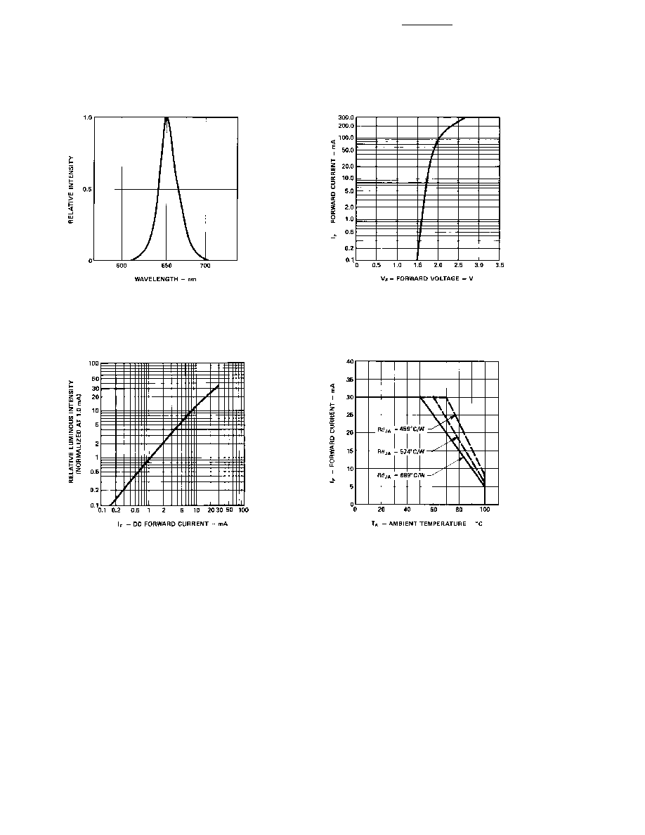
Notes:
1. Maximum I
PEAK
at f = 1 kHz, DF = 6.7%.
2. Derate linearly as shown in Figure 4.
3. The transient peak current is the maximum non-recurring peak current the device can withstand without damaging the LED die and
wire bonds. It is not recommended that the device be operated at peak currents beyond the Absolute Maximum Peak Forward Current.
Electrical/Optical Characteristics at T
A
= 25
∞
C
Symbol
Description
Min.
Typ.
Max.
Unit
Test Condition
V
F
Forward Voltage
1.6
1.8
V
I
F
= 1 mA
V
R
Reverse Breakdown Voltage
5.0
15.0
V
I
R
= 100
µ
A
p
Peak Wavelength
645
nm
Measurement at Peak
d
Dominant Wavelength
637
nm
Note 1
1
/
2
Spectral Line Halfwidth
20
nm
S
Speed of Response
30
ns
Exponential Time
Constant, e
-t
/T
S
C
Capacitance
30
pF
V
F
= 0, f = 1 MHz
R
J-PIN
Thermal Resistance
260
[3]
∞
C/W
Junction to Cathode Lead
210
[4]
290
[5]
V
Luminous Efficacy
80
Im/W
Note 2
Notes:
1. The dominant wavelength,
d
, is derived from the CIE chromaticity diagram and represents the color of the device.
2. The radiant intensity, I
e
, in watts per steradian, may be found from the equation I
e
= l
V
/
V
, where I
V
is the luminous intensity in
candelas and
V
is luminous efficacy in lumens/watt.
3. HLMP-D150.
4. HLMP-D155.
5. HLMP-K150/-K155.