Agilent HMMC-1015
DC≠50 GHz Variable Attenuator
Data Sheet
Description
The HMMC-1015 is a monolithic,
voltage variable, GaAs IC attenu-
ator that operates from DC to
50 GHz. The distributed topology
of the HMMC-1015 minimizes the
parasitic effects of its series and
shunt FETs, allowing the
HMMC-1015 to exhibit a wide
dynamic range across its full
bandwidth. An on-chip DC
reference circuit may be used to
maintain optimum VSWR for any
attenuation setting or to improve
the attenuation versus voltage
linearity of the attenuator circuit.
Features
∑ Specified Frequency Range:
DC≠26.5 GHz
∑ P
in
(-1dB):
27 dBm @ 500 MHz
∑ Return Loss:
10 dB
∑ Minimum Attenuation:
2.0 dB
∑ Maximum Attenuation:
30.0 dB
Absolute Maximum Ratings
[1]
Symbol
Parameters/Conditions
Units
Min.
Max.
V
DC-RF
DC Voltage to RF Ports
V
-0.6
+1.6
V
1
V
1
Control Voltage
V
-10.5
+0.5
V
2
V
2
Control Voltage
V
-10.5
+0.5
V
DC
DC In/DC Out
V
-0.6
+1.0
P
IN
RF Input Power
dBm
17
T
mina
Min. Ambient Operating Temp.
∞
C
-55
T
maxa
Max. Ambient Operating Temp.
∞
C
+125
T
stg
Storage Temperature
∞
C
-65
+165
T
max
Max. Assembly Temp. (for 60 sec. max.)
∞
C
+300
Note:
1. Operation in excess of any one of these conditions may result in damage to this device.
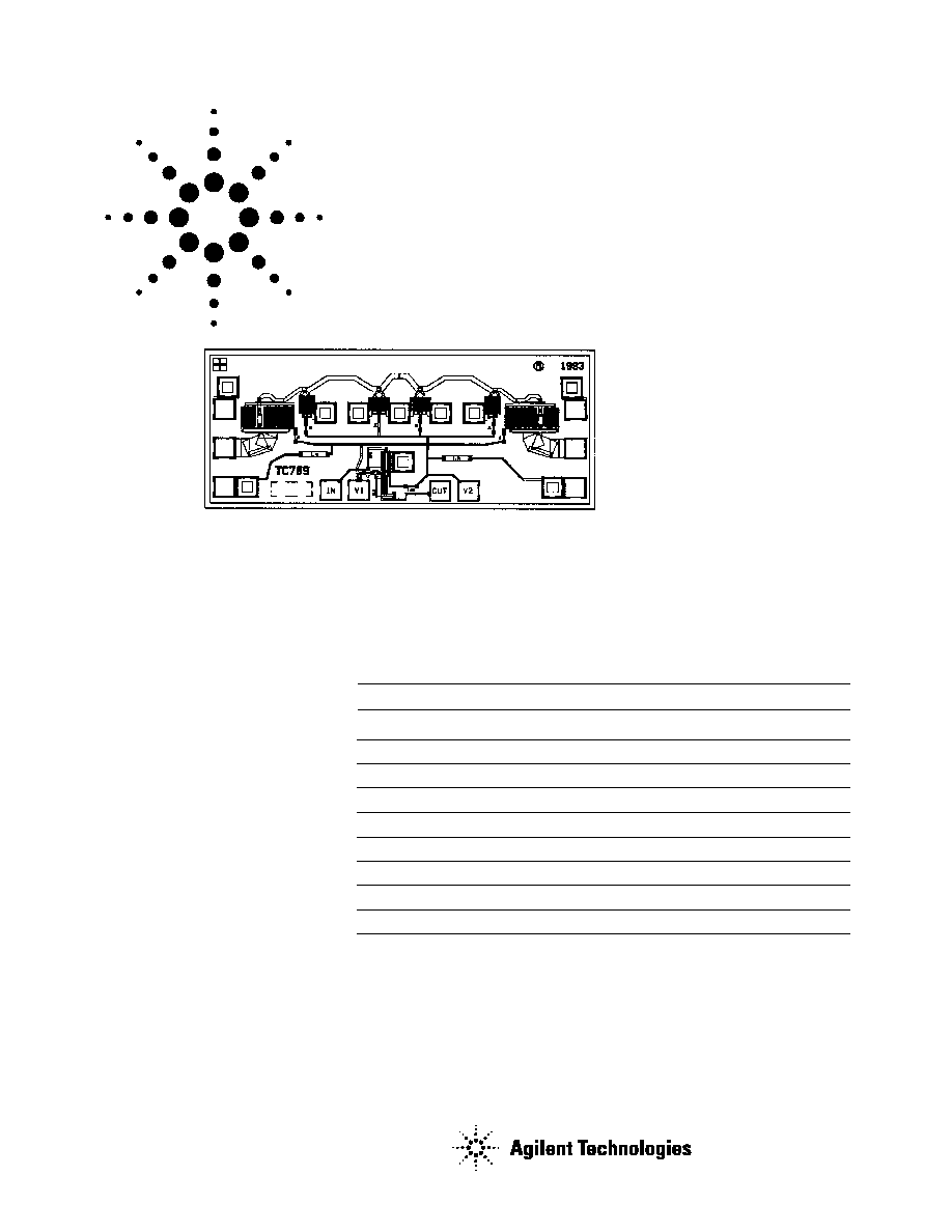
Chip Size:
1470 x 610
µ
m (57.9 x 24.0 mils)
Chip Size Tolerance:
±
10
µ
m (
±
0.4 mils)
Chip Thickness:
127
±
15
µ
m (5.0
±
0.6 mils)

2
HMMC-1015 DC Specifications/Physical Properties, T
A
= 25
∞
C
Symbol
Parameters and Test Conditions
Units
Min.
Typ.
Max.
I
V1
V
1
Control Current, (V
1
= -10V)
mA
5.0
5.9
7.1
I
V2
V
2
Control Current, (V
2
= -10V)
mA
5.0
5.9
7.1
V
P
Pinch-Off Voltage
V
-6.75
-5.0
-3.75
Electrical Specifications
[1]
, T
A
= 25
∞
C, Z
O
= 50
Parameters and Test Conditions
Units
Freq.
Min.
Typ.
Max.
(GHz)
1.5
1.0
2.4
8.0
1.4
2.4
Minimum Attenuation, |S
21
| (V
1
= 0 V, V
2
= -10 V)
dB
20.00
1.7
2.4
26.5
2.0
2.4
50.0
3.9
Input/Output Return Loss @ Min. Attenuation Setting,
dB
<26.5
10
16
(V
1
= 0 V, V
2
= -10 V)
<50.0
8
1.5
27
30
8.0
27
38
Maximum Attenuation, |S
21
| (V
1
= -10 V, V
2
= 0 V)
dB
20.0
27
38
26.5
27
40
50.0
35
P
-1dB
@ Minumum Attenuation
dBm
300 kHz
18.5
dBm
>500 MHz
27
Input/Output Return Loss @ Max. Attenuation Setting,
dB
<26.5
8
10
(V
1
= -10V, V
2
= 0V)
dB
<50.0
10
DC Power Dissipation, V
1
= -10.5 V, V
2
= -10.5 V
mW
158
(does not include input signals)
Note:
1. Attenuation is a positive number; whereas, S
21
as measured on a Network Analyzer would be a negative number.
3
Application
The HMMC-1015 is designed to be
used as a gain control block in an
ALC assembly. Because of its wide
dynamic range and return loss
performance, the HMMC-1015 may
also be used as a broadband pulse
modulator or single-pole single-
throw, non-reflective switch.
Operation
The attenuation value of the
HMMC-1002 is adjusted by apply-
ing negative voltage to V
2
. At any
attenuation setting, optimum
VSWR is obtained by applying
negative voltage to V
1
. Applying
negative voltage (V
2
) to the gates
of the shunt FETs sets the
source-to-drain resistance and
establishes the attenuation level.
Applying negative voltage (V
1
) to
the gates of the series FETs opti-
mizes the input and output
match for different attenuation
settings. In some applications, a
single setting of V
1
may provide
sufficient input and output
match over the desired attenua-
tion range (V
2
). For any
HMMC-1015 the values of V
1
may
be adjusted so that the device
attenuation versus voltage is
monotonic for both V
1
and V
2
;
however, this will slightly de-
grade the input and output
return loss.
The attenuation and input/
output match of the HMMC-1015
may also be controlled using only
a single input voltage by utilizing
the on-chip DC reference circuit
and the driver circuit shown in
Figure 4. This circuit optimizes
VSWR for any attenuation
setting. Because of process
variations, the values of V
REF
,
R
REF
, and R
L
are different for
each wafer if optimum perfor-
mance is required. Typical values
for these elements are given. The
ratio of the resistors R
1
and R
2
determines the sensitivity of the
attenuation versus voltage
performance of the attenuator.
For more information on the
performance of the HMMC-1015
and the driver circuits previously
mentioned see MWTC's Applica-
tion Note #37, "HMMC-1021
Attenuator: Attenuation Con-
trol." For more S-parameter
information, see MWTC's Appli-
cation Note #44, "HMMC-1015
Attenuator: S-Parameters."
Assembly Techniques
GaAs MMICs are ESD sensitive.
ESD preventive measures must
be employed in all aspects of
storage, handling, and assembly.
MMIC ESD precautions, handling
considerations, die attach and
bonding methods are critical
factors in successful GaAs MMIC
performance and reliability.
Agilent application note #54,
"GaAs MMIC ESD, Die Attach
and Bonding Guidelines" pro-
vides basic information on these
subjects.
V
1
50
50
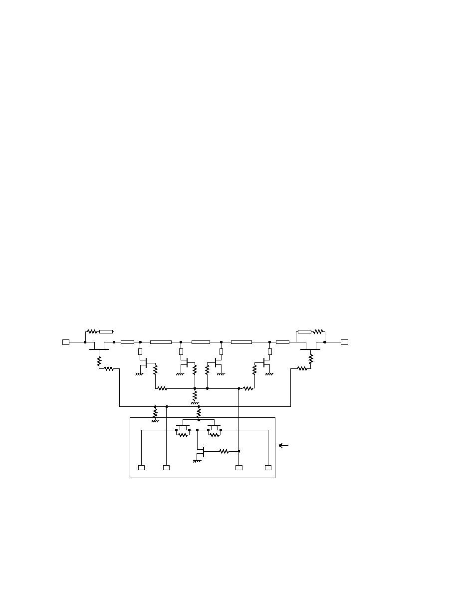
RF Attenuator Circuit
50
500
500
DC
IN
DC
OUT
500
DC Reference Circuit
V
2
RF
IN
RF
OUT
Figure 1. HMMC-1015 Schematic.
4
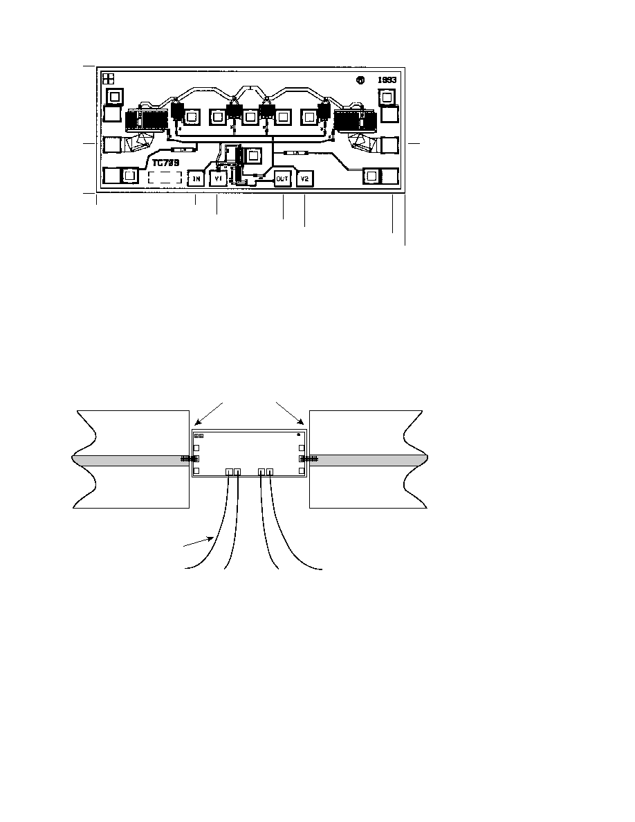
Figure 2. HMMC-1015 Bonding Pad Locations.
RF
OUT
RF
IN
DC
IN
DC
OUT
V
1
V
2
4 Wire Bonds using 0.7 mil dia.
Gold Bond Wire
(length NOT important)
2.0 mil
nom. gap
TC721R
Figure 3. HMMC-1015 Assembly Diagram.
610
0
233
233
476
0
584
887
994
1410
1470
Notes:
1. All dimensions in microns and shown to center of bond pad.
2. DC
in
, V
1
, DC
out
, and V
2
bonding pads are 75 x 75 microns.
3. RF input and output bonding pads are 60 x 70 microns.
4. Chip thickness: 127
±
15
µ
m.
5
V
REF
500
(350
≠ 500
)
500
Op. Amp
A
B
(-0.4 V to -1.0 V)
V
IN
(0 V to -10.0 V)
R
REF
To
DC
IN
To
V
1
To
V
2
(400
≠ 500
)
R
L
To
DC
OUT
≠
+
Figure 4. Attenuator Driver.
HMMC-1015 Typical Performance
Figure 5. Attenuation vs. Frequency.
[1]
1
3
5
7
9
11
13
15
17
19
21
23
25
27
FREQUENCY (GHz)
ATTENUATION (dB)
60
50
40
30
20
10
0
Figure 6. Output Return Loss vs. Frequency.
[1]
1
3
5
7
9
11
13
15
17
19
21
23
25
27
FREQUENCY (GHz)
RETURN LOSS (dB)
60
50
40
30
20
10
0
Maximum
Attenuation
Minimum
Attenuation
Note:
1. Data obtained from on-wafer measurements. T
chuck
= 25
∞
C.