 | ÐлекÑÑоннÑй компоненÑ: HMMC-2006 | СкаÑаÑÑ:  PDF PDF  ZIP ZIP |
Äîêóìåíòàöèÿ è îïèñàíèÿ www.docs.chipfind.ru
7-20
DC 6 GHz Unterminated SPDT
Switch
Technical Data
HMMC-2006
Features
· Frequency Range: DC-6 GHz
· Insertion Loss:
<1dB @ 6 GHz
· Isolation:
>70 dB @ 45 MHz
>35 dB @ 6 GHz
· Return Loss: >12 dB
(Both Input & Output)
· Switching Speed: <1 ns
· P
-1dB
:
23 dBm @ 50 MHz
>27dBm @ 6 GHz
· Harmonics: <-25 dBc @
20 dBm (DC coupled)
Description
The HMMC-2006 is a GaAs
monolithic microwave integrated
circuit (MMIC) designed for low
insertion loss and high isolation
from DC to 6 GHz. It is intended
for use as a general-purpose,
singlepole, double-throw (SPDT)
switch. One series and two shunt
MESFETs per throw provide
1.2 dB maximum insertion loss
and 35 dB minimum isolation at
6 GHz. HMMC-2006 chips use
through-substrate vias to provide
ground connections to the chip
backside and minimize the
number of wire bonds required.
The HMMC-2006 is also available
in an 8-lead flatpack (1GG7-4201).
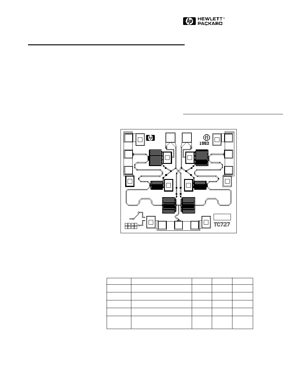
Chip Size:
960 x 1070
µ
m (37.8 x 42.1 mils)
Chip Size Tolerance:
+0, -10
µ
m (+0, -0.4 mils)
Chip Thickness:
127
±
15
µ
m (5.0
±
0.6 mils)
Pad Dimensions:
80 x 80
µ
m (3.2 x 3.2 mils), or larger
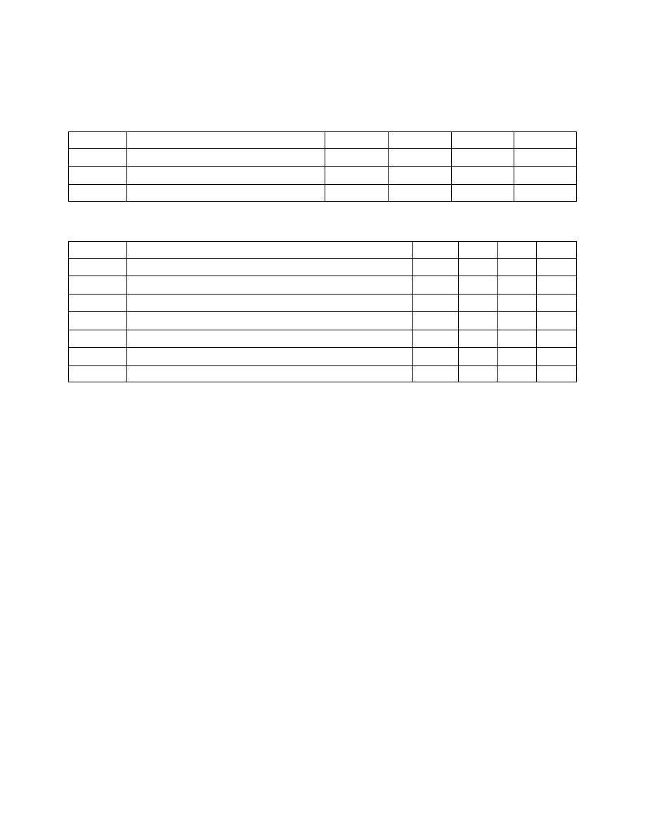
Absolute Maximum Ratings
[1]
Symbol
Parameters/Conditions
Units
Min.
Max.
V
sel
Select Voltages 1 and 2
V
-12
+3
P
in
RF Input Power
dBm
30
T
op
Operating Temperature
°
C
-55
+125
T
STG
Storage Temperature
°
C
-65
+165
T
max
Maximum Assembly Temp.
°
C
+300
(for 60 seconds max.)
Note:
1. Operation in excess of any one of these conditions may result in permanent
damage to this device. T
A
= 25
°
C except for T
ch
, T
STG
, and T
max
.
SEL1
SEL2
RF
OUT1
RF
IN
RF
OUT2
Chip ID
5965-9071E
7-21
DC Specifications/Physical Properties,
T
A
= 25
°
C
Symbol
Parameters and Test Conditions
Units
Min.
Typ.
Max.
I
l
Leakage Current @ -10 V
µ
A
100
V
p
Pinch-off Voltage @ 8 mA
V
-6.75
-3.25
BV
gss
Breakdown Voltage Total
V
-18.0
-12.5
RF Specifications,
T
A
= 25
°
C, Z
O
= 50
, V
sel
high = 0 V, V
sel
low = -10 V
Symbol
Parameters and Test Conditions
Units
Min.
Typ.
Max.
BW
Guaranteed Operating Bandwidth
GHz
DC
6
IL
Insertion Loss, RF
in
to RF
out
,
f = 6 GHz, ON throw
dB
1
1.2
ISO
Isolation, RF
in
to RF
out
,
f = 6 GHz, OFF throw
dB
35
40
RL
in
Input Return Loss
dB
12
14
RL
out
Output Return Loss
dB
12
15
P
1 dB
Input Power where IL increases by 1 dB
f = 50 MHz
dBm
18
23
t
s
Switching Speed, 10% 90% RF Envelope,
f = 2 GHz
ns
1

7-22
Applications
The HMMC-2006 can be used in
instrumentation, communica-
tions, radar, ECM, EW, and many
other systems requiring SPDT
switching. It can be used for
pulse modulation, port isolation,
transfer switching, high-speed
switching, replacement of me-
chanical switches, and so on. It
can also be used as a terminated
SPST (single-pole-single-throw)
switch by placing a 50
load on
either RF output port.
Assembly Techniques
Die attach may be done with
either a AuSn solder preform or
conductive epoxy. Gold
thermosonic bonding is recom-
mended for all bonds. The top
and bottom metallization is gold.
For more detailed information
see HP application note #999
"GaAs MMIC Assembly and
Handling Guidelines."
GaAs MMICs are ESD sensitive.
Proper precautions should be used
when handling these devices.
S-Parameters
[1]
,
T
A
= 25
°
C, Z
O
= 50
, V
sel
high
= 0 V, V
sel
low
= -10 V
Frequency
S
11
S
21
(Insertion Loss)
S
31
(Isolation)
GHz
Mag.
Ang.
Mag.
Ang.
Mag.
Ang.
0.1
0.93
-8
4.26
172
0.01
86
0.5
0.0365
-27.03
0.9366
-11.32
0.0010
78.03
1.0
0.0372
-41.81
0.9336
-17.35
0.0017
76.84
1.5
0.0448
-63.14
0.9311
-23.47
0.0026
76.05
2.0
0.0542
-80.60
0.9286
-27.67
0.0033
75.66
2.5
0.0631
-88.46
0.9271
-29.73
0.0039
77.4
3.0
0.0715
-93.98
0.9242
-33.03
0.0049
81.14
3.5
0.0795
-101.90
0.9199
-38.93
0.0059
82.09
4.0
0.0872
-108.90
0.9164
-45.14
0.0063
78.90
4.5
0.0951
-114.40
0.9123
-50.49
0.0068
78.94
5.0
0.1022
-120.90
0.9054
-56.36
0.0078
84.68
5.5
0.1074
-123.50
0.9032
-62.07
0.0084
84.71
6.0
0.1138
-132.70
0.9058
-69.04
0.0115
91.24
Note:
1. 3-port-wafer-probed data.
7-23
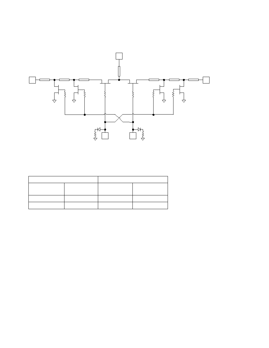
SEL2
RF
OUT
RF
OUT
RF IN
SEL2
Figure 1. HMMC-2006 Schematic.
Recommended Operating Conditions,
T
A
= 25
°
C
Select Line
RF Path
RF IN to
RF IN to
SEL1
SEL2
RF OUT1
RF OUT2
-10 V
0 V
Isolated
Low Loss
0 V
-10 V
Low Loss
Isolated
7-24
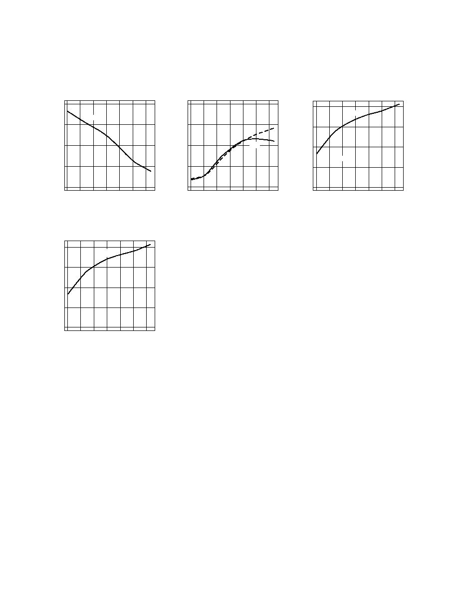
HMMC-2006 Typical Performance
0
2
4
6
FREQUENCY (GHz)
Figure 2. Insertion Loss
[1]
vs.
Frequency.
-80
-60
-70
-50
-40
0
2
4
6
-80
-60
-70
-50
-40
0
2
4
6
-30
-22
-26
-18
-14
INSERTION LOSS (dB)
FREQUENCY (GHz)
Figure 5. Output-to-Output Isolation
[2]
vs. Frequency.
ISOLATION (dB)
FREQUENCY (GHz)
Figure 3. Input and Output (On
Throw) Return Loss
[1]
vs. Frequency.
RETURN LOSS (dB)
FREQUENCY (GHz)
Figure 4. Input-to-Output Isolation
[1]
vs. Frequency.
ISOLATION (dB)
S
21-ON
S
11
S
22
S
21-ON
S
21-OFF
0
2
4
6
-80
-60
-70
-50
-40
S
23
Notes:
1. Wafer-probed measurements
2. Calculated from wafer-probed measurements
Document Outline
- List of Figures
- 1. HMMC-2006 Schematic.
- 2. Insertion Loss [1] vs.
- 3. Input and Output (On
- 4. Input-to-Output Isolation [1]
- 5. Output-to-Output Isolation [2]
- 6. HMMC-2006 Bonding Pad Locations. (Dimensions in micrometers)
- Features
- Description
- Absolute Maximum Ratings [1]
- DC Specifications/Physical Properties, T A = 25°C
- RF Specifications, T A = 25°C, Z O = 50 W, V sel high = 0 V, V sel low = -10 V
- Applications
- Assembly Techniques
- S-Parameters [1] , TA =25°C, ZO = 50 W, Vsel high = 0 V, Vsel low = -10 V
- Recommended Operating Conditions, TA =25°C
- HMMC-2006 Typical Performance