 | ÐлекÑÑоннÑй компоненÑ: HMMC-2027 | СкаÑаÑÑ:  PDF PDF  ZIP ZIP |
Äîêóìåíòàöèÿ è îïèñàíèÿ www.docs.chipfind.ru
7-32
DC 26.5 GHz SPDT GaAs MMIC
Switch
Technical Data
HMMC-2027
Features
· Outputs Terminated in 50
When Off
· Frequency Range:
DC- 26.5 GHz
· Insertion Loss:
2.5dB @ 26.5 GHz
· Isolation: >70 dB @ 45 MHz
30 dB @ 26.5 GHz
· Return Loss:
15 dB (Both Input and Selected
Output)
12 dB Unselected Output
· Switching Speed:
<1 ns (10%-90% RF)
· P
-1dB
: 18 dBm @ 10 MHz
27 dBm @ 2 GHz
· Harmonics (DC Coupled):
<-45 dBc @ 10 MHz and 5 dBm
<-65 dBc @ 2 GHz and 5 dBm
Description
The HMMC-2027 is a GaAs
monolithic microwave integrated
circuit (MMIC) designed for low
insertion loss and high isolation
from DC to 26.5 GHz. It is
intended for use as a general-
purpose, single-pole, double-
throw (SPDT), absorptive switch.
Two series and two shunt
MESFETs per throw provide 3 dB
maximum insertion loss and
30 dB minimum isolation at
26.5 GHz. HMMC-2027 chips use
through-substrate vias to provide
ground connections to the chip
backside and minimize the
number of wire bonds required.
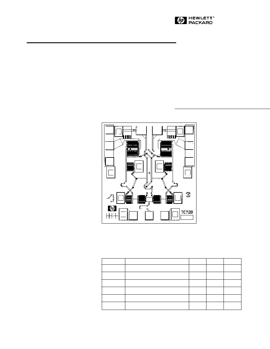
Chip Size:
900 x 960
µ
m (35.4 x 37.8 mils)
Chip Size Tolerance:
±
10
µ
m (
±
0.4 mils)
Chip Thickness:
127
±
15
µ
m (5.0
±
0.6 mils)
Pad Dimensions:
80 x 80
µ
m (3.2 x 3.2 mils), or larger
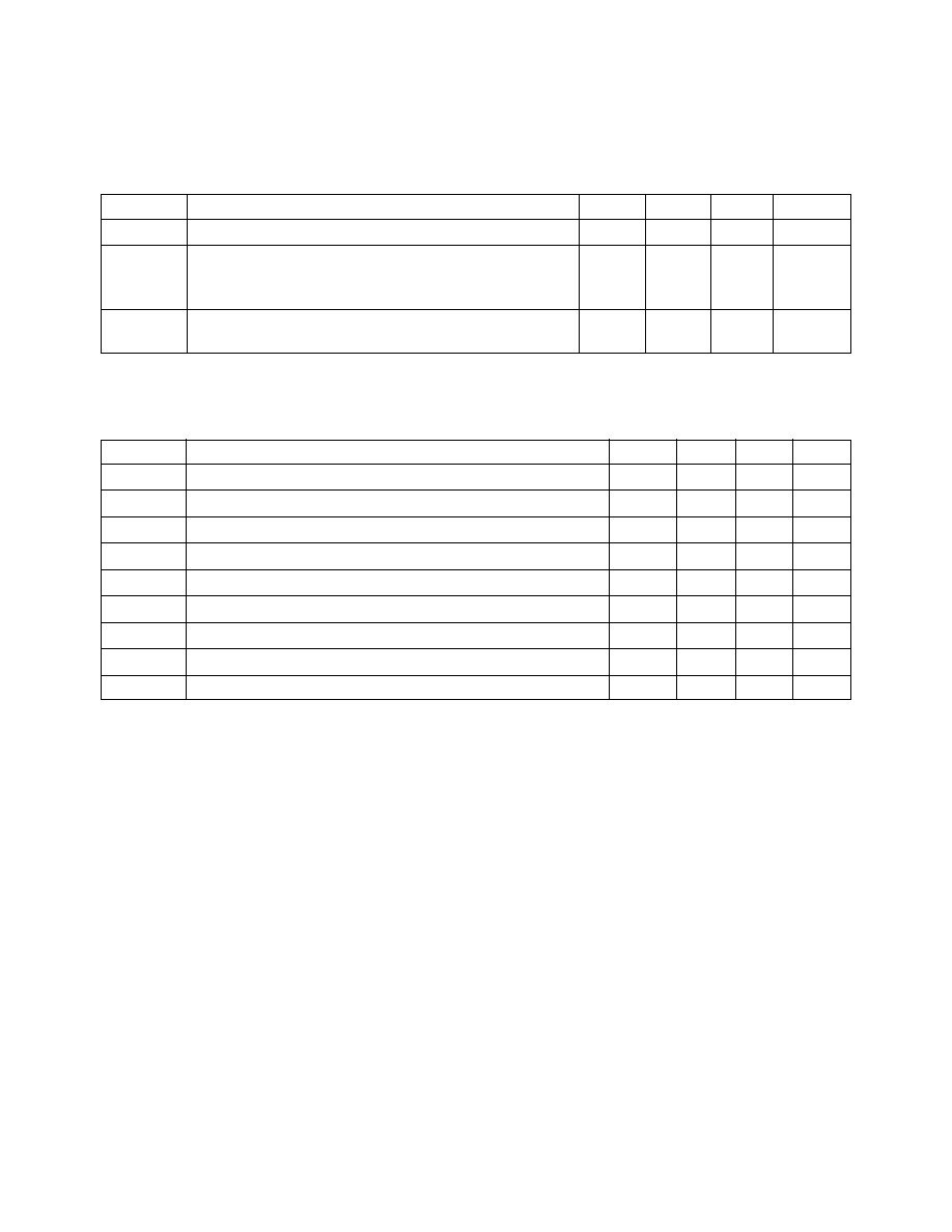
Absolute Maximum Ratings
[1]
Symbol
Parameters/Conditions
Units
Min.
Max.
V
sel
Select Voltages 1 and 2
V
-10.5
+3
P
in
RF Input Power
dBm
25
T
op
Operating Temperature
°
C
-55
+125
T
STG
Storage Temperature
°
C
-65
+165
T
max
Maximum Assembly Temp.
°
C
+200
P
unsel
[2]
Power into Unselected Output
dBm
15
Notes:
1. Operation in excess of any one of these conditions may result in permanent
damage to this device. T
A
= 25
°
C except for T
op
, T
STG
, and T
max
.
2. Operation in excess of these @ T
op-max
may result in permanent damage.
RF
IN
RF
OUT2
CHIP ID
RF
OUT1
SEL1
SEL2
5965-5450E
7-33
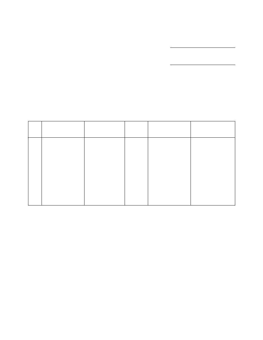
DC Specifications/Physical Properties,
T
A
= 25
°
C
Symbol
Parameters and Test Conditions
Units
Min.
Typ.
Max.
I
l
Leakage Current @ -10 V
µ
A
200
Pinch-Off Voltage (V
SEL2
= V
p
, V
RFout2
= +2 V,
V
p
I
RFout2
= 2 mA, V
SEL1
= -10 V, V
RFout1
= open circuit,
V
-6.75
-3.00
V
RFin
= GND
BV
gss
Breakdown Voltage (Test FET w/V
D
= V
S
= GND,
I
G
= -50
µ
A)
V
-13.0
RF Specifications,
T
A
= 25
°
C, Z
O
= 50
, V
sel-high
= 0 V, V
sel-low
= -10 V
Symbol
Parameters and Test Conditions
Units
Min.
Typ.
Max.
BW
Guaranteed Operating Bandwidth
GHz
DC
26.5
IL
Insertion Loss, RF
in
to Selected RF
out
,f = 26.5 GHz, ON throw
dB
2.5
3.0
ISO
Isolation, RF
in
to Unselected RF
out
,f = 26.5 GHz, OFF throw
dB
27
30
ISO
Isolation, RF
in
to Unselected RF
out
, f = 18 GHz, OFF throw
dB
40
43
RL
in
Input Return Loss
dB
12
15
RL
out-ON
Output Return Loss, ON throw
dB
13
16
RL
out-OFF
Output Return Loss, OFF throw
dB
9
12
P
1 dB
Input Power where IL increases by 1 dB
f
in
= 2 GHz
dBm
27
t
s
Switching Speed, 10% 90% RF Envelope
f
in
= 2 GHz
ns
1
7-34
Applications
The HMMC-2027 can be used in
instrumentation, communica-
tions, radar, ECM, EW, and many
other systems requiring SPDT
switching. It can be used for
pulse modulation, port isolation,
transfer switching, high-speed
switching, replacement of
mechanical switches, and so on.
Assembly Techniques
Die attach should be done with
conductive epoxy. Gold
thermosonic bonding is recom-
mended for all bonds. The top
and bottom metallization is gold.
For more detailed information
see HP application note #999,
"GaAs MMIC Assembly and
Handling Guidelines."
GaAs MMICs are ESD sensitive.
Proper precautions should be used
when handling these devices.
S-Parameters
[1]
,
T
A
= 25
°
C, Z
O
= 50
, V
sel
high
= 0 V, V
sel
low
= -10 V
Freq.
S
11
S
21
S
31
S
22
S
33
GHz
(Insertion Loss)
(Isolation)
(ON Throw)
(OFF Throw)
dB
Mag.
Ang.
dB
Mag. Ang.
dB
dB
Mag.
Ang.
dB
Mag.
Ang.
0.5
-26.41 0.048
-57.11
-1.08
0.88
-49.06
-67.74
-28.40
0.03
-47.94
-32.26
0.024
47.18
0.5
-18.28
0.12
-7.04
-1.33
0.86
-8.52
-71.40
-18.44
0.12
-9.89
-16.79
0.14
173.87
1.5
-18.53
0.12
-13.70
-1.35
0.86
-14.62
-61.02
-18.46
0.12
-19.75
-16.47
0.15
171.75
4.0
-18.92
0.11
-27.64
-1.41
0.85
-24.53
-51.67
-18.75
0.12
-38.78
-15.36
0.17
168.03
6.5
-19.43
0.11
-45.02
-1.47
0.84
-39.56
-49.50
-19.10
0.11
-63.22
-14.55
0.19
152.55
9.0
-20.57
0.09
-64.07
-1.56
0.84
-55.13
-46.87
-19.72
0.10
15.79
-14.28
0.19
136.68
11.5
-21.85
0.08
-2.59
-1.62
0.83
-71.03
-44.71
-20.91
0.09
243.63
-13.84
0.20
121.81
14.0
-23.10
0.07
258.44
-1.74
0.82
-29.63
-42.30
-22.41
0.08
217.48
-13.53
0.21
106.44
16.5
-24.05
0.06
235.82
-1.88
0.81
258.60
-41.74
-24.17
0.06
179.74
-12.95
0.23
92.94
19.0
-24.59
0.06
224.56
-1.99
0.80
242.13
-37.07
-27.09
0.04
133.20
-12.76
0.23
74.01
21.5
-25.42
0.05
206.39
-2.10
0.79
227.84
-40.39
-28.85
0.04
68.10
-13.12
0.22
68.84
24.0
-24.66
0.06
209.77
-2.10
0.78
209.72
-34.46
-24.31
0.06
6.26
-12.11
0.25
54.32
26.5
-21.90
0.08
223.86
-2.39
0.76
191.82
-31.38
-19.43
0.11
-33.31
-12.03
0.25
38.26
Note:
1. Three-port-wafer-probed data: Port 1 = RF Input, Port 2 = Selected RF Output (i.e., ON throw), and Port 3 = Unselected
RF Output (i.e., OFF throw).
7-35
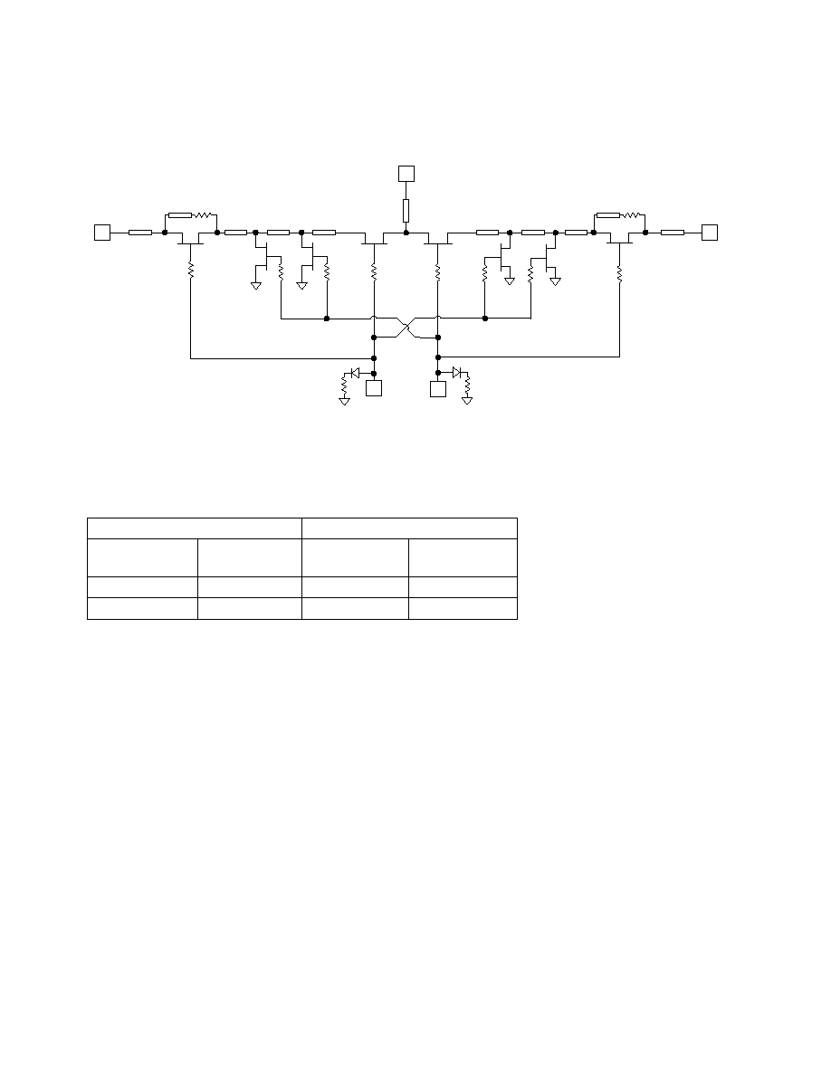
RF
OUT1
RF
OUT2
RF IN
SEL1
SEL2
Figure 1. HMMC-2027 Schematic.
Recommended Operating Conditions,
T
A
= 25
°
C
Select Line
RF Path
RF IN to
RF IN to
SEL1
SEL2
RF OUT1
RF OUT2
-10 V
0 V
Isolated
Low Loss
0 V
-10 V
Low Loss
Isolated
7-36
HMMC-2027 Typical Performance
Notes:
1. Data obtained from wafer-probed measurements.
2. All compression and harmonic data measured on individual device mounted
in an HP83040 Series Modular Microcircuit Package @ T
case
= 25
°
C.
3. Harmonic data points below -80 dBc are at or near the noise floor of the
measurement system.
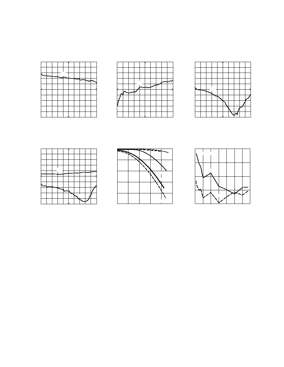
0.045
26.5
FREQUENCY (GHz)
Figure 2. Insertion Loss
[1]
vs.
Frequency.
-5
-3
-4
-2
-1
0
0.045
26.5
-100
-60
-80
-40
-20
0
INSERTION LOSS (dB)
Figure 5. Output Return Loss
[1]
vs.
Frequency.
FREQUENCY (GHz)
Figure 3. Input-to-Output Isolation
[1]
vs. Frequency.
ISOLATION (dB)
Figure 4. Input Return Loss
[1]
vs.
Frequency.
0.045
26.5
-40
-24
-32
-16
-8
0
FREQUENCY (GHz)
INPUT RETURN LOSS (dB)
S
21
S
31
S
11
0.045
26.5
-30
-18
-24
-12
-6
0
FREQUENCY (GHz)
OUTPUT RETURN LOSS (dB)
Figure 6. Gain Compression
[2]
vs.
Power Input.
17
21
27
25
23
19
-5
-3
-4
-2
-1
0
POWER INPUT (dBm)
GAIN COMPRESSION (dB)
S
33
S
22
3 GHz
1 GHz
300 MHz
100 MHz
50 MHz
Figure 7. Harmonics vs.
Fundamental Frequency
[2,3]
.
0
2
7
6
3
1
-90
-70
-80
-60
-50
FUNDAMENTAL FREQUENCY (GHz)
HARMONICS (dBc)
5
4
Second
Third
P
in
= 5 dBm
Document Outline
- List of Figures
- 1. HMMC-2027 Schematic.
- 2. Insertion Loss [1] vs. Frequency
- 3. Input-to-Output Isolation [1] vs. Frequency
- 4. Input Return Loss [1] vs. Frequency
- 5. Output Return Loss [1] vs. Frequency
- 6. Gain Compression [2] vs. Power Input.
- 7. Harmonics vs. Fundamental Frequency.
- 8. HMMC-2027 Bonding Pad Locations. (Dimensions in micrometers)
- Features
- Description
- Absolute Maximum Ratings [1]
- DC Specifications/Physical Properties, T A = 25°C
- RF Specifications, T A = 25°C, Z O = 50 W, V sel-high = 0 V, V sel-low = -10 V
- Applications
- Assembly Techniques
- S-Parameters [1] , TA =25°C, ZO = 50 W, Vsel high = 0 V, Vsel low = -10 V
- Recommended Operating Conditions, TA =25°C
- HMMC-2027 Typical Performance