 | –≠–ª–µ–∫—Ç—Ä–æ–Ω–Ω—ã–π –∫–æ–º–ø–æ–Ω–µ–Ω—Ç: HMMC-3028 | –°–∫–∞—á–∞—Ç—å:  PDF PDF  ZIP ZIP |
6-31
Description
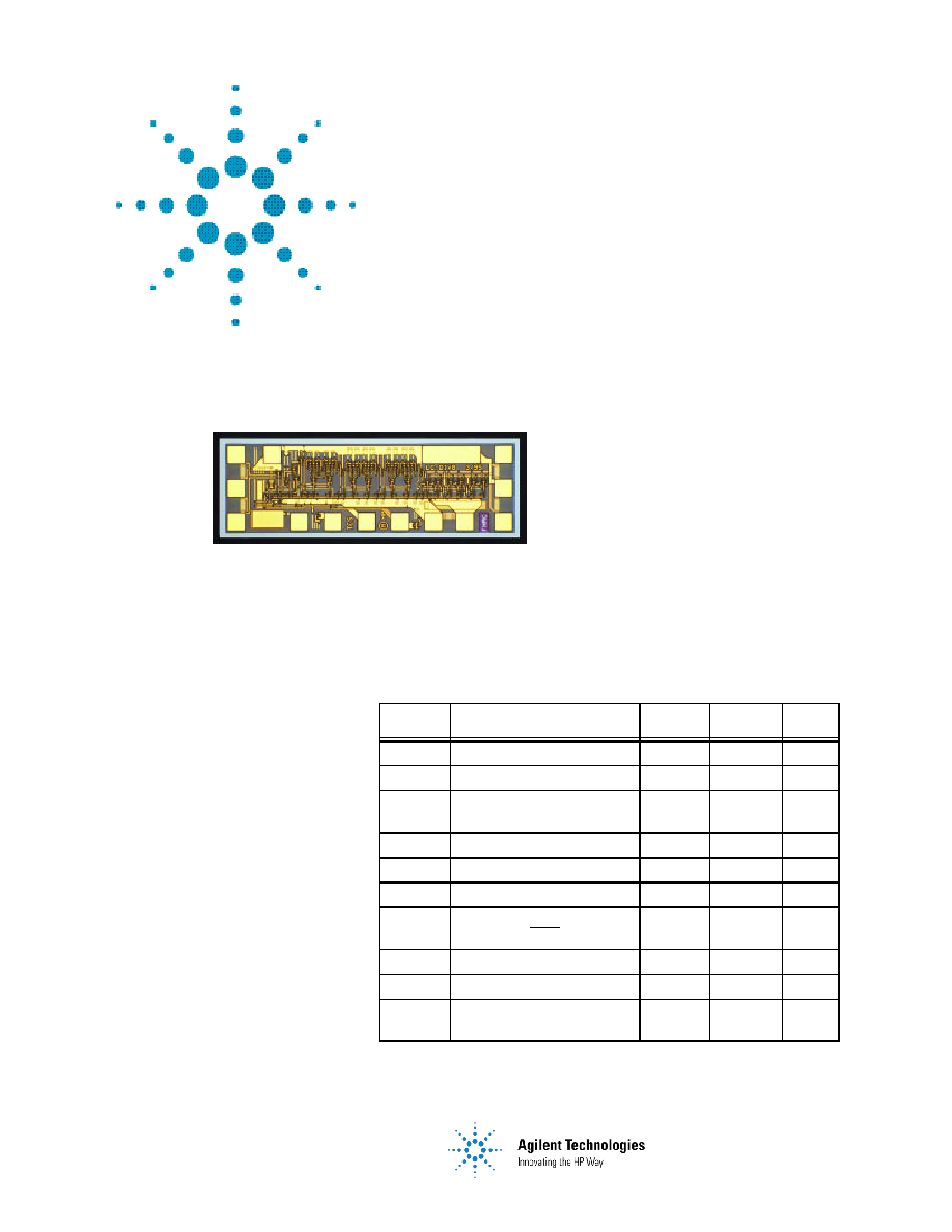
The HMMC-3028 GaAs HBT MMIC
Prescaler offers DC to 12 GHz fre-
quency translation for use in commu-
nications and EW systems
incorporating high-frequency PLL os-
cillator circuits and signal-path down
conversion applications. The prescal-
er provides a large input power sensi-
tivity window and low phase noise. In
addition to the features listed above
the device offers an input disable
contact pad to eliminate any self-
oscillation condition.
Agilent HMMC-3028
DC - 12 GHz High Efficiency
GaAs HBT MMIC
Divide-by-8 Prescaler
Data Sheet
Chip Size:
1330
◊
440
µ
m (52.4
◊
17.3 mils)
Chip Size Tolerance:
±
10
µ
m (
±
0.4 mils)
Chip Thickness:
127
±
15
µ
m (5.0
±
0.6 mils)
Pad Dimensions:
70
◊
70
µ
m (2.8
◊
2.8 mils)
Absolute Maximum Ratings
[1]
(@ T
A
=25
∞
C, unless otherwise indicated)
[1]
Operation in excess of any parameter limit (except T
BS
) may cause permanent dam-
age to the device.
Symbol
Parameters/Conditions
Min.
Max.
Units
V
CC
Bias Supply Voltage
+7
volts
V
EE
Bias Supply Voltage
-7
volts
|V
CC
-
V
EE
|
Bias Supply Delta
+7
volts
V
Disable
Pre-amp Disable Voltage
V
EE
V
CC
volts
V
Logic
Logic Threshold Voltage
V
CC
-1.5
V
CC
-1.2
volts
P
in(CW)
CW RF Input Power
+10
dBm
V
RFin
DC Input Voltage
(@ RFin or RFin Ports)
V
CC
±
0.5
volts
T
BS
[2]
[2]
MTTF >4x10
5
hours @ T
BS
<85
∞
C. Operation in excess of maximum operating tem-
perature (T
BS
) will degrade MTTF.
Backside Operating Temp
-40
+85
∞
C
T
st
Storage Temperature
-65
+165
∞
C
T
max
Maximum Assembly Temp.
(60 seconds max.)
310
∞
C
Features
∑ Wide Frequency Range:
0.2 - 12 GHz
∑ High Input Power Sensitivity:
On-chip pre- and post-amps
-20 to +10 dBm (1 - 8 GHz)
-15 to +10 dBm (8 - 10 GHz)
-10 to +5 dBm (10 - 12 GHz)
∑ Dual-mode P
out
: (Chip Form)
0 dBm [0.5 V
p-p
] @ 44 mA
-6.0 dBm [0.25 V
p-p
] @ 34 mA
∑ Low Phase Noise:
-153 dBc/Hz @ 100 kHz Offset
∑ (+) or (-) Single Supply Bias
Operation
∑ Wide Bias Supply Range:
4.5 to 6.5 volt operating range
∑ Differential I/0 with on-chip
50
matching
6-32
HMMC-3028/rev.3.X
RF Specifications
(T
A
= 25
∞
C, Z
0
= 50
,
V
CC
- V
EE
= 5.0 volts)
HMMC-3028
(
˜
8)
Symbol
Parameters/Conditions
Min.
Typ.
Max.
Units
in(max)
Maximum input frequency of operation
12
14
GHz
in(min)
Minimum input frequency of operation
[1]
(P
in
= - 10 dBm)
[1]
For sine-wave input signal. Prescaler will operate down to D.C. for square-wave input signal. Minimum divide frequency limited by in-
put slew-rate.
0.2
0.5
GHz
Self-Osc.
Output Self-Oscillation Frequency
[2]
[2]
Prescaler may exhibit this output signal under bias in the absence of an RF input signal. This condition may be eliminated by use of the
Pre-amp Disable (V
Disable
) feature, or the Differential Input de-biasing technique.
1.7
GHz
P
in
@ DC, (Square-wave input)
-15
>-25
+10
dBm
@
in
=500 MHz, (Sine-wave input)
-15
>-20
+10
dBm
in
=1 to 8 GHz
-15
>-20
+10
dBm
in
=8 to 10 GHz
-10
>-15
+5
dBm
in
=10 to 12 GHz
-5
>-10
-1
dBm
RL
Small-Signal Input/Output Return Loss
(@
in
<
12
GHz)
15
dB
S
12
Small-Signal Reverse Isolation (@
in
<
12
GHz)
30
dB
N
SSB Phase noise (@ P
in
= 0 dBm, 100kHz offset
from a
out
= 1.2 GHz Carrier
-153
dBc/Hz
Jitter
Input signal time variation @ zero-crossing
(
in
=10 GHz, P
in
= -10 dBm)
1
ps
r
or
f
Output Edge speed (10% to 90% rise/fall time)
70
ps
DC Specifications/Physical Properties
(T
A
= 25
∞
C, V
CC
- V
EE
= 5.0 volts, unless otherwise listed)
HMMC-3028
Symbol
Parameters/Conditions
Min.
Typ.
Max.
Units
V
CC
- V
EE
Operating bias supply difference
[1]
[1]
Prescaler will operate over full specified supply voltage range. V
CC
or V
EE
not to exceed limits specified in Absolute Maximum Ratings
section.
4.5
5.0
6.5
volts
|I
CC
| or |I
EE
|
Bias supply current
(
HIGH Output Power Configuration
[2]
: V
Pwr-
Sel
=V
EE
)
[2]
High output power configuration: P
out
= 0 dBm [V
out
= 0.5 V
p-p
], Low output power configuration: P
out
= -6.0 dBm [V
out
= 0.25 V
p-p
].
37
44
51
mA
Bias supply current
(
LOW Output Power Configuration: V
PwrSel
=open)
29
34
39
mA
V
RFin(q)
V
RFout(q)
Quiescent DC voltage appearing at all RF ports
V
CC
volts
V
Logic
Nominal ECL Logic Level
(V
Logic
contact self-bias voltage, generated on-
chip)
V
CC
- 1.45
V
CC
-1.32
V
CC
-1.25
volts
HMMC-3028/rev.3.X
6-33
RF Specifications (Cont.'d)
(T
A
= 25
∞
C, Z
0
= 50
, V
CC
- V
EE
= 5.0 volts)
HMMC-3028
High Output Power
Operating Mode
[1]
[1]
V
PwrSel
=V
EE
.
Symbol
Parameters/Conditions
Min.
Typ.
Max.
Units
P
out
@
out
<
1 GHz,
-2.0
0
dBm
@
out
=1.25 GHz
-2.0
0
dBm
@
out
=1.5 GHz
-2.25
-0.25
dBm
|V
out(p-p)
|
@
out
<1 GHz,
0.39
0.5
volts
@
out
=1.25 GHz
0.39
0.5
volts
@
out
=1.5 GHz
0.38
0.48
volts
P
Spitback
out
power level appearing at RFin or RFin
(@
in
10 GHz, Unused RFout or RFout
unterminated.
-61
dBm
out
power level appearing at RFin or RFin
(@
in
=10 GHz, Both RFout & RFout
terminated.
-81
dBm
P
feedthru
Power
level of
in
appearing at RFout or RFout
(@
in
=12 GHz, P
in
=0 dBm, Referred to P
in
(
in
))
-30
dBc
H
2
Second harmonic distortion output level
(@
out
=1.5 GHz, Referred to P
out
(
out
))
-30
dBc
Low Output Power
Operating Mode
[2]
[2]
V
PwrSel
=Open Circuit.
P
out
@
out
<
1 GHz,
-8.0
-6.0
dBm
@
out
=1.25 GHz
-8.0
-6.0
dBm
@
out
=1.5 GHz
-8.25
-6.25
dBm
|V
out(p-p)
|
@
out
<1 GHz,
0.20
0.25
volts
@
out
=1.25 GHz
0.20
0.25
volts
@
out
=1.5 GHz
0.19
0.24
volts
P
Spitback
out
power level appearing at RFin or RFin
(@
in
10 GHz, Unused RFout or RFout
unterminated.
-71
dBm
out
power level appearing at RFin or RFin
(@
in
=10 GHz, Both RFout & RFout
terminated.
-91
dBm
P
feedthru
Power
level of
in
appearing at RFout or RFout
(@
in
=12 GHz, P
in
=0 dBm, Referred to P
in
(
in
))
-30
dBc
H
2
Second harmonic distortion output level
(@
out
=1.5 GHz, Referred to P
out
(
out
))
-35
dBc
V
CC
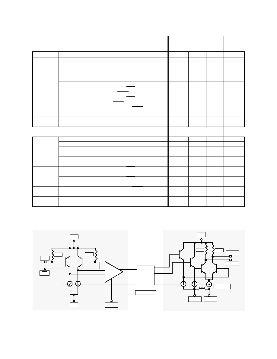
Figure 1.
Simplified Schematic
18/36 mA
V
EE
V
EE
RFout
RFin
RFout
RFin
Divide Cell
Post Amplifier Stage
Input Preamplifier Stage
50
V
PwrSel
V
Disable
V
CC
˜
8
50
50
50

6-34
HMMC-3028/rev.3.X
all power dissipation. (NOTE:
V
EE
must ALWAYS be bonded
and V
PwrSel
must NEVER be
biased to any potential other
than V
EE
or open-circuited.)
2)V
Logic
ECL Contact Pad
Under normal conditions no
connection or external bias is
required to this pad and it is
self-biased to the on-chip ECL
logic threshold voltage (V
CC
-
1.35 v). The user can provide
an external bias to this pad (1.5
to 1.2 volts less than V
CC
) to
force the prescaler to operate
at a system generated logic
threshold voltage.
3)Input Disable Feature
If an RF signal with sufficient
signal to noise ratio is present
at the RF input, the prescaler
will operate and provide a di-
vided output equal to the input
frequency divided by the divide
modulus. Under certain "ideal"
conditions where the input is
well matched at the right input
frequency, the device may
"self-oscillate", especially un-
der small signal input powers
or with only noise present at
the input This "self-oscillation"
will produce a undesired out-
put signal also known as a false
trigger. By applying an exter-
nal bias to the input disable
contact pad (more positive
than V
CC
- 1.35v), the input
preamplifier stage is locked
into either logic "high" or logic
"low" preventing frequency di-
vision and any self-oscillation
frequency which may be
present.
4)Input DC Offset
Another method used to pre-
vent false triggers or self-
oscillation conditions is to ap-
ply a 20 to 100 mV DC offset
voltage between the RFin and
RFin ports. This prevents noise
or spurious low level signals
from triggering the divider.
Applications
The HMMC-3028 is designed for
use in high frequency communi-
cations, microwave instrumenta-
tion, and EW radar systems
where low phase-noise PLL con-
trol circuitry or broad-band fre-
quency translation is required.
Operation
The device is designed to operate
when driven with either a single-
ended or differential sinusoidal
input signal over a 200 MHz to 12
GHz bandwidth. Below 200 MHz
the prescaler input is "slew-rate"
limited, requiring fast rising and
falling edge speeds to properly
divide. The device will operate at
frequencies down to DC when
driven with a square-wave.
The device may be biased from
either a single positive or single
negative supply bias. The back-
side of the device is not DC con-
nected to any DC bias point on
the device.
For positive supply operation
V
CC
is nominally biased at any
voltage in the +4.5 to +6.5 volt
range with V
EE
(or V
EE
& V
Pwr-
Sel
) grounded. For negative bias
operation V
CC
is typically
grounded and a negative voltage
between -4.5 to -6.5 volts is ap-
plied to V
EE
(or V
EE
& V
PwrSel
).
Several features are designed
into this prescaler:
1)Dual-Output Power Fea-
ture
Bonding both V
EE
and V
PwrSel
pads to either ground (positive
bias mode) or the negative
supply (negative bias mode),
will deliver ~0 dBm [0.5 V
p-p
]
at the RF output port while
drawing ~40 mA supply cur-
rent. Eliminating the V
PwrSel
connection results in reduced
output power and voltage
swing, -6.0 dBm [0.25 V
p-p
] but
at a reduced current draw of
~30 mA resulting in less over-
Adding a 10K
resistor be-
tween the unused RF input to a
contact point at the V
EE
poten-
tial will result in an offset of
25mV between the RF inputs.
Note however, that the input
sensitivity will be reduced
slightly due to the presence of
this offset
Assembly Techniques
Figure 3 shows the chip assembly
diagram for single-ended I/O op-
eration through 12 GHz for either
positive or negative bias supply
operation. In either case the sup-
ply contact to the chip must be
capacitively bypassed to provide
good input sensitivity and low in-
put power feedthrough. Indepen-
dent of the bias applied to the
device, the backside of the chip
should always be connected to
both a good RF ground plane and
a good thermal heat sinking re-
gion on the mounting surface.
All RF ports are DC connected
on-chip to the V
CC
contact
through on-chip 50
resistors.
Under any bias conditions where
VCC is not DC grounded, the RF
ports should be AC coupled via
series capacitors mounted on the
thin-film substrate at each RF
port. Only under bias conditions
where V
CC
is DC grounded (as is
typical for negative bias supply
operation) may the RF ports be
direct coupled to adjacent cir-
cuitry or in some cases, such as
level shifting to subsequent stag-
es. In the latter case the device
backside may be "floated" and
bias applied as the difference be-
tween V
CC
and V
EE
.
All bonds between the device and
this bypass capacitor should be
as short as possible to limit the in-
ductance. For operation at fre-
quencies below 1 GHz, a large
value capacitor must be added to
provide proper RF bypassing.
Due to on-chip 50
matching re-
sistors at all four RF ports, no ex-
ternal termination is required on
HMMC-3028/rev.3.X
6-35
RFin
RFin
RFout
RFout
V
CC
V
EE
V
Disable
V
Logic
V
PwrSel
V
CC
V
CC
V
CC
0 70
350 500 650 800 950 1090
1260 1330
0
70
220
370
440
900
230
260
Figure 2.
Pad Locations & Chip Dimensions
Notes:
∑ All dimensions in microns.
∑ All Pad Dim: 70 x 70
µ
m
(except where noted).
∑ Tolerances:
±
10
µ
m
∑ Chip Thickness: 127
±
15
µ
m
No
V
CCBypass
any unused RF port. However,
improved "Spitback" perfor-
mance (~ 20 dB) and input sensi-
tivity can be achieved by
terminating the unused RFout
port to V
CC
through 50
(positive
supply) or to ground via a 50
termination (negative supply op-
eration).
GaAs MMICs are ESD sensitive.
ESD preventive measures must
be employed in all aspects of
storage, handling, and assembly.
MMIC ESD precautions, handling
considerations, die attach and
bonding methods are critical fac-
tors in successful GaAs MMIC
performance and reliability.
Agilent application note #54,
"GaAs MMIC ESD, Die Attach
and Bonding Guidelines" pro-
vides basic information on these
subjects.
Connection
Optional DC Operating Values / Logic Levels
(T
A
= 25
∞
C)
Function
Symbol
Conditions
Min.
(volts/mA)
Typical
(volts/mA)
Max.
(volts/mA)
Logic
Threshold
[1]
[1]
Acceptable voltage range when applied from external source.
V
Logic
V
CC
-1.5
V
CC
-1.35
V
CC
-1.2
Input
Disable
V
Disable(High)
[Disable]
V
Logic
+ 0.25
V
Logic
V
CC
V
Disable(Low)
[Enable]
V
EE
V
Logic
- 0.25
I
Disable
V
D
> V
EE
+3
(V
Disable
-V
EE
- 3) / 500
V
D
< V
EE
+3
0