 | –≠–ª–µ–∫—Ç—Ä–æ–Ω–Ω—ã–π –∫–æ–º–ø–æ–Ω–µ–Ω—Ç: HMMC-5027 | –°–∫–∞—á–∞—Ç—å:  PDF PDF  ZIP ZIP |
Document Outline
- List of Figures
- 1. HMMC-5027 Schematic.
- 2. HMMC-5027 Bonding Pad Locations.
- 3. HMMC-5027 Assembly Diagram
- 4. Typical Gain and Reverse Isolation vs. Frequency
- 5. Typical Input and Output Return Loss vs. Frequency
- 6. Typical Small-Signal Gain vs. Temperature
- 7. Typical Gain vs. Second Gate Control Voltage
- 8. Typical 1 dB Gain Compression and Saturated Output Power vs. Frequency
- 9. Typical Second and Third Harmonic vs. Fundamental Frequency
- 10. Typical Noise Figure Performance
- Features
- Description
- Absolute Maximum Ratings
- HMMC-5027 DC Specifications/Physical Properties
- HMMC-5027 RF Specifications
- HMMC-5027 Applications
- Biasing and Operation
- Assembly Techniques
- HMMC-5027 Typical Performance
- Typical Scattering Parameters
- HMMC-5027 Typical Performance
6-47
H
2 ≠ 26.5 Medium Power Amplifier
Technical Data
Features
∑ Wide-Frequency Range:
2 - 26.5 GHz
∑ Moderate Gain: 7 dB
∑ Gain Flatness: 1 dB
∑ Return Loss:
Input
-13 dB
Output
-11 dB
∑ Low-Frequency Operation
Capability: < 2 GHz
∑ Gain Control:
30 dB Dynamic Range
∑ Medium Power:
20 GHz:
P
-1dB
: 22 dBm
P
sat
:
24 dBm
26.5 GHz:
P
-1dB
: 19 dBm
P
sat
:
21 dBm
Description
The HMMC-5027 is a broadband
GaAs MMIC Traveling Wave
Amplifier designed for medium
output power and moderate gain
over the full 2 to 26.5 GHz
frequency range. Seven MESFET
cascode stages provide a flat gain
response, making the HMMC-5027
an ideal wideband power block.
Optical lithography is used to
produce gate lengths of
0.5 mm.
The HMMC-5027 incorporates
advanced MBE technology,
Ti-Pt-Au gate metallization,
silicon nitride passivation, and
polyimide for scratch protection.
Chip Size:
2980 x 770
µ
m (117.3 x 30.3 mils)
Chip Size Tolerance:
±
10
µ
m (
±
0.4 mils)
Chip Thickness:
127
±
15
µ
m (5.0
±
0.6 mils)
Pad Dimensions:
75 x 75
µ
m (2.95 x 2.95 mils), or larger
HMMC-5027
Absolute Maximum Ratings
[1]
Symbol
Parameters/Conditions
Units
Min.
Max.
V
DD
Positive Drain Voltage
V
8.0
I
DD
Total Drain Current
mA
300
V
G1
First Gate Voltage
V
-5
0
I
G1
First Gate Current
mA
-1
+1
V
G2
Second Gate Voltage
V
-2.5
+5
I
G2
Second Gate Current
mA
-25
P
DC
DC Power Dissipation
watts
2.4
P
in
CW Input Power
dBm
23
T
ch
Operating Channel Temp.
∞
C
+150
T
case
Operating Case Temp.
∞
C
-55
T
STG
Storage Temperature
∞
C
-65
+165
T
max
Maximum Assembly Temp.
∞
C
+300
(for 60 seconds maximum)
Note:
1. Operation in excess of any one of these conditions may result in permanent
damage to this device. T
A
= 25
∞
C except for T
ch
, T
STG
, and T
max
.
5965-5447E

6-48
HMMC-5027 DC Specifications/Physical Properties
[1]
Symbol
Parameters and Test Conditions
Units
Min.
Typ.
Max.
I
DSS
Saturated Drain Current
mA
200
300
500
(V
DD
= 8.0 V, V
G1
= 0.0 V, V
G2
= open circuit)
V
p
First Gate Pinch-off Voltage
V
-2.2
-1.3
-.5
(V
DD
= 8.0 V, I
DD
= 30 mA, V
G2
= open circuit)
V
G2
Second Gate Self-Bias Voltage
V
1.8
(V
DD
= 8.0 V, V
G1
= 0.0 V)
(0.27 x V
DD
)
I
DSOFF
(V
G1
)
First Gate Pinch-off Current
mA
7
(V
DD
= 8.0 V, V
G1
= -3.5 V, V
G2
= open circuit)
I
DSOFF
(V
G2
)
Second Gate Pinch-off Current
mA
10
(V
DD
= 5.0 V, V
G1
= 0.0 V, V
G2
= -3.5 V)
ch-bs
Thermal Resistance (T
backside
= 25
∞
C)
∞
C/W
28
Note:
1. Measured in wafer form with T
chuck
= 25
∞
C. (Except
ch-bs
.)
HMMC-5027 RF Specifications
[1]
,
T
op
= 25
∞
C, V
D1
= V
D2
= 5 V, V
G1
= V
G2
= Open, Z
O
= 50
, unless otherwise noted
Symbol
Parameters and Test Conditions
Units
Min.
Typ.
Max.
BW
Guaranteed Bandwidth
[2]
GHz
2
26.5
S
21
Small Signal Gain
dB
6
7
S
21
Small Signal Gain Flatness
dB
±
0.8
RL
in
Input Return Loss
dB
-13
-10
RL
out
Output Return Loss
dB
-11
-10
S
12
Reverse Isolation
dB
-28
-25
P
-1dB
Output Power @ 1dB Gain Compression
dBm
16.5
19
P
sat
Saturated Output Power
dBm
18.5
21
H
2
Second Harmonic Power Level (2 <
o
< 20)
dBc
-21
-18
[P
o
(
o
) = 21 dBm or P
-1dB
, whichever is less]
H
3
Third Harmonic Power Level (2 <
o
< 20)
dBc
-32
-18
[P
o
(
o
) = 21 dBm or P
-1dB
, whichever is less]
NF
Noise Figure
dB
11
Notes:
1. Small-signal data measured in wafer form with T
chuck
= 25
∞
C. Large-signal data measured on individual devices
mounted in an HP83040 Series Modular Microcircuit Package at T
A
= 25
∞
C.
2. Performance may be extended to lower frequencies through the use of appropriate off-chip circuitry. Upper corner
frequency ~ 30 GHz.
6-49
HMMC-5027 Applications
The HMMC-5027 series of travel-
ing wave amplifiers are designed
for use as general purpose
wideband power stages in
communication systems and
microwave instrumentation. They
are ideally suited for broadband
applications requiring a flat gain
response and excellent port
matches over a 2 to 26.5 GHz
frequency range. Dynamic gain
control and low-frequency
extension capabilities are
designed into these devices.
Biasing and Operation
These amplifiers are biased with
a single positive drain supply
(V
DD
) and a single negative gate
supply (V
G1
). The recommended
bias conditions for the
HMMC-5027 are V
DD
= 8.0V,
I
DD
= 250 mA or I
DSS
, whichever is
less. To achieve this drain current
level, V
G1
is typically biased
between 0 V and -0.6 V. No other
bias supplies or connections to
the device are required for 2 to
26.5 GHz operation. The gate
voltage (V
G1
) MUST be applied
prior to the drain voltage (V
DD
)
during power up and removed
after the drain voltage during
power down. See Figure 3 for
assembly information.
The auxiliary gate and drain
contacts are used only for low-
frequency performance extension
below
1.0 GHz. When used,
these contacts must be AC
coupled only. (Do not attempt to
apply bias to these pads.)
The second gate (V
G2
) can be
used to obtain 30 dB (typical)
dynamic gain control. For normal
operation, no external bias is
required on this contact and its
self-bias potential is between +1.5
and +2.5 volts. Applying an
external bias between its open
circuit potential and -2.5 volts will
adjust the gain while maintaining
a good input/output port match.
Assembly Techniques
Solder die-attach using a fluxless
AuSu solder preform is the
recommended assembly method.
Gold thermosonic wedge bonding
with 0.7 mil diameter Au wire is
recommended for all bonds. Tool
force should be 22
±
1 gram, stage
temperature should be 150
±
2
∞
C,
and ultrasonic power and dura-
tion should be 64
±
1 dB and
76
±
8 msec, respectively. The
bonding pad and chip backside
metallization is gold.
For more detailed information
see HP application note #999
"GaAs MMIC Assembly and
Handling Guidelines."
GaAs MMICs are ESD sensitive.
Proper precautions should be used
when handling these devices.
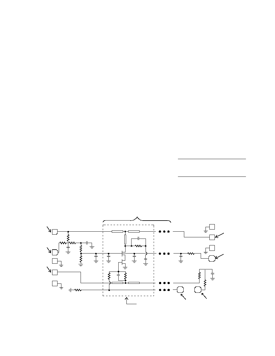
Figure 1. HMMC-5027 Schematic.
Aux. Drain
Drain Bias
(V
DD
)
RF Input
Single Stage Shown
First Gate
Bias (V
G1
)
Second Gate
Bias (V
G2
)
RF Output
Aux. Gate
Notes:
FET gate periphery in microns.
All resistors in ohms. (
),
(or in K-ohms, where indicated)
Seven Identical Stages
50
248
248
17K
15K
30K
7.5
5.5
50

6-50
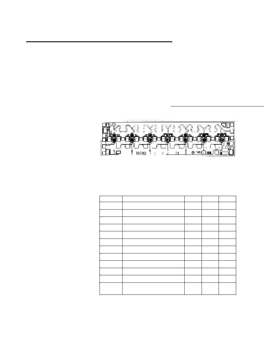
Figure 2. HMMC-5027 Bonding Pad Locations.
Figure 3. HMMC-5027 Assembly Diagram.
V
DD
(V
DD
and Aux Drain Pads)
(V
G2
Pad)
(RF Input Pad)
Aux.
Drain
RF
Input
700
70
Chip ID No.
Aux. Gate
V
G1
V
G2
RF
Output
770
(
±
10
µ
m)
75
285
555
2910
2900
2580
2290
70
(RF Output Pad)
2980 (
±
10
µ
m)
465
220
0
Notes:
All dimensions in microns.
Rectangular Pad Dim: 75 x 75
µ
m.
Octagonal Pad Dim: 90
µ
m dia.
All other dimensions
±
5
µ
m (unless otherwise noted).
Chip thickness: 127
±
15
µ
m.
V
DD
V
G1
OUT
IN
1.5 mil dia.Gold Wire
Bond to
15 nF
DC Feedthru
4 nH Inductor
(1.0 mil Gold Wire Bond
with length of 200 mils)
0.7 mil dia. Gold Bond Wire
(Length NOT important)
Gold Plated Shim
68 pF Capacitor
Input and Output Thin Film
Circuit with
8 pF
DC Blocking Capacitor
2.0 mil
nom. gap
2.0 mil
nom. gap
Trace Offset
168
µ
m
(6.6 mils)
1.5 mil dia.Gold Wire
Bond to
15 nF DC Feedthru
Bonding Island
Trace Offset
168
µ
m
(6.6 mils)
Note:
Total offset between RF input and RF
output pad is 335
µ
m (13.2 mils).
6-51
HMMC-5027 Typical Performance
Typical Scattering Parameters
[1]
,
(T
chuck
= 25
∞
C, V
DD
= 8.0 V, I
DD
= 250 mA or I
DSS
, whichever is less, Z
in
= Z
o
= 50
Freq.
S
11
S
21
S
12
S
22
GHz
dB
Mag
Ang
dB
Mag
Ang
dB
Mag
Ang
dB
Mag
Ang
2.0
-18.7
0.116
-139.5
-57.7
0.0013 -165.2
8.7
2.717
116.6
-13.0
0.223
173.5
3.0
-20.1
0.099
-159.0
-54.9
0.0018 144.2
8.4
2.635
94.8
-13.0
0.224
150.0
4.0
-21.5
0.084
-175.7
-52.0
0.0025 154.0
8.3
2.612
72.0
-13.5
0.212
127.1
5.0
-24.6
0.059
167.8
-49.9
0.0032 111.3
8.4
2.634
48.2
-14.0
0.200
101.6
6.0
-32.0
0.025
167.4
-48.2
0.0039 91.3
8.6
2.699
23.3
-15.3
0.171
71.7
7.0
-30.8
0.029
-94.8
-46.9
0.0045 74.9
8.8
2.763
-3.5
-16.9
0.143
39.5
8.0
-22.7
0.073
-103.2
-45.5
0.0053 21.0
8.8
2.768
-30.9
-18.4
0.120
-2.2
9.0
-18.9
0.114
-121.5
-45.2
0.0055 10.3
8.8
2.744
-58.9
-21.3
0.086
-46.9
10.0
-17.2
0.137
-142.6
-44.7
0.0058 -15.5
8.5
2.673
-85.9
-18.9
0.114
-90.7
11.0
-17.4
0.135
-163.9
-43.5
0.0067 -33.4
8.3
2.608
-112.5
-17.9
0.127
-129.6
12.0
-19.3
0.108
175.6
-41.5
0.0084 -45.4
8.2
2.564
-138.5
-18.2
0.123
-162.6
13.0
-25.6
0.052
170.3
-40.6
0.0093 -75.8
8.2
2.578
-164.9
-19.3
0.108
163.4
14.0
-27.0
0.045
-113.0
-38.6
0.0118 -95.9
8.3
2.610
167.1
-22.1
0.078
126.5
15.0
-19.2
0.109
-111.0
-37.8
0.0129 -124.7
8.3
2.605
138.4
-31.2
0.028
56.7
16.0
-15.6
0.167
-127.9
-37.1
0.0139 -149.1
8.2
2.574
108.8
-23.5
0.067
-33.3
17.0
-14.3
0.193
-148.4
-36.3
0.0153 -174.5
8.0
2.510
79.7
-18.1
0.124
-80.7
18.0
-14.8
0.182
-166.6
-35.8
0.0163 164.1
7.8
2.444
50.9
-15.2
0.174
-115.2
19.0
-17.1
0.140
-179.3
-34.7
0.0185 141.5
7.7
2.418
22.1
-13.7
0.207
-147.6
20.0
-21.4
0.086
-166.2
-32.9
0.0227 112.6
7.8
2.466
-7.5
-13.9
0.202
177.9
21.0
-18.4
0.121
-129.5
-31.6
0.0262 80.7
8.1
2.527
-39.9
-16.8
0.145
136.7
22.0
-13.8
0.205
-137.2
-30.9
0.0285 42.7
8.0
2.512
-74.0
-25.3
0.054
66.9
23.0
-12.1
0.247
-152.7
-30.6
0.0296 13.3
7.6
2.395
-108.4
-19.8
0.102
-56.2
24.0
-12.3
0.244
-169.8
-30.3
0.0304 -15.5
7.4
2.344
-142.5
-13.7
0.207
-103.5
25.0
-14.7
0.184
-175.8
-29.7
0.0329 -44.9
7.3
2.315
-175.6
-11.3
0.272
-136.7
26.0
-16.7
0.146
-149.3
-28.5
0.0375 -78.1
7.9
2.469
148.1
-11.7
0.259
-171.3
26.5
-14.1
0.197
-141.6
-28.0
0.0399 -98.5
8.0
2.503
126.9
-13.0
0.223
172.3
Note:
1. Data obtained from on-wafer measurements.
2
4
6
10
8
14 16 18
12
24 26.5
22
20
FREQUENCY (GHz)
V
DD
= 8.0 V, I
DD
= 250 mA
[1]
V
DD
= 8.0 V, I
DD
= 250 mA
[1]
Figure 4. Typical Gain and Reverse
Isolation vs. Frequency.
10
9
8
7
6
5
4
3
2
1
0
≠10
≠20
≠30
≠40
≠50
≠60
SMALL-SIGNAL GAIN, S
21
(dB)
REVERSE ISOLATION, S
12
(dB)
OUTPUT RETURN LOSS,S
22
(dB)
2
4
6
10
8
14 16 18
12
24 26.5
22
20
FREQUENCY (GHz)
Figure 5. Typical Input and Output
Return Loss vs. Frequency.
≠10
≠15
≠20
≠25
≠30
≠35
≠40
≠10
≠15
≠20
≠25
≠30
≠35
≠40
INPUT RETURN LOSS, S
11
(dB)