Document Outline
- HMPP-389x Series
- Description/Applications
- Features
- Pin Connections and Package Marking
- Package Lead Code Identification
- Absolute Maximum Ratings
- Electrical Specifications
- Typical Parameters
- Typical Performance
- Typical Applications
- Applications Information
- PIN Diodes
- Diode Construction
- Diode Lifetime and Its Implications
- Diode Resistance vs. Forward Bias
- Linear Equivalent Circuit
- Testing the HMPP-389T on the Demo-board
- Demo-board Preparation
- Test Results
- Assembly Information
- SMT Assembly
- MiniPak Outline Drawing
- Ordering Information
- Device Orientation
- Tape Dimensions and Product Orientation

Agilent HMPP-389x Series
MiniPak Surface Mount
RF PIN Switch Diodes
Data Sheet
Description/Applications
These ultra-miniature products
represent the blending of Agilent
Technologies' proven semiconduc-
tor and the latest in leadless
packaging technology.
The HMPP-389x series is optimized
for switching applications where
low resistance at low current and
low capacitance are required. The
MiniPak package offers reduced
parasitics when compared to
conventional leaded diodes, and
lower thermal resistance.
Features
∑ Surface mount MiniPak package
≠ low height, 0.7 mm (0.028") max.
≠ small footprint, 1.75 mm
2
(0.0028 inch
2
)
∑ Better thermal conductivity for
higher power dissipation
∑ Single and dual versions
∑ Matched diodes for consistent
performance
∑ Low capacitance
∑ Low resistance at low current
∑ Low FIT (Failure in Time) rate*
∑ Six-sigma quality level
* For more information, see the Surface
Mount Schottky Reliability Data Sheet.
Pin Connections and
Package Marking
3
2
Product code
Date code
4
AA
1
Package Lead Code Identification
(Top View)
Single
3
2
4
1
#0
Anti-parallel
3
2
4
1
#2
Parallel
3
2
4
1
#5
Shunt Switch
3
2
4
1
T
Anode
Cathode
Cathode
Anode
Low junction capacitance of the
PIN diode chip, combined with
ultra low package parasitics, mean
that these products may be used
at frequencies which are higher
than the upper limit for conven-
tional PIN diodes.
Note that Agilent's manufacturing
techniques assure that dice
packaged in pairs are taken from
adjacent sites on the wafer,
assuring the highest degree of
match.
The HMPP-389T low inductance
wide band shunt switch is well
suited for applications up to 6 GHz.
Notes:
1. Package marking provides orientation and
identification.
2. See "Electrical Specifications" for
appropriate package marking.

2
HMPP-389x Series Absolute Maximum Ratings
[1]
, T
C
= 25
∞
C
Symbol
Parameter
Units
Value
I
f
Forward Current (1
µ
s pulse)
Amp
1
P
IV
Peak Inverse Voltage
V
100
T
j
Junction Temperature
∞
C
150
T
stg
Storage Temperature
∞
C
-65 to +150
jc
Thermal Resistance
[2]
∞
C/W
150
Notes:
1. Operation in excess of any one of these conditions may result in permanent damage to the
device.
2. T
C
= +25
∞
C, where T
C
is defined to be the temperature at the package pins where contact is
made to the circuit board.
Electrical Specifications, T
C
= +25
∞
C, each diode
Part Number
Package
Minimum Breakdown
Maximum Series
Maximum Total
HMPP-
Marking Code
Lead Code
Configuration
Voltage (V)
Resistance
(
)
Capacitance (pF)
3890
D
0
Single
100
2.5
0.30
3892
C
2
Anti-parallel
3895
B
5
Parallel
389T
T
T
Shunt Switch
Test Conditions
V
R
= V
BR
I
F
= 5 mA
V
R
= 5 V
Measure I
R
10
µ
A
f = 100 MHz
f = 1 MHz
ESD WARNING:
Handling Precautions Should Be
Taken To Avoid Static Discharge.
Typical Parameters, T
C
= +25
∞
C
Part Number
Series Resistance
Carrier Lifetime
Total Capacitance
HMPP-
R
S
(
)
(ns)
C
T
(pF)
389x
3.8
200
0.20 @ 5 V
Test Conditions
I
F
= 1 mA
I
F
= 10 mA
f = 100 MHz
I
R
= 6 mA

3
HMPP-389x Series Typical Performance, T
c
= 25
∞
C, each diode
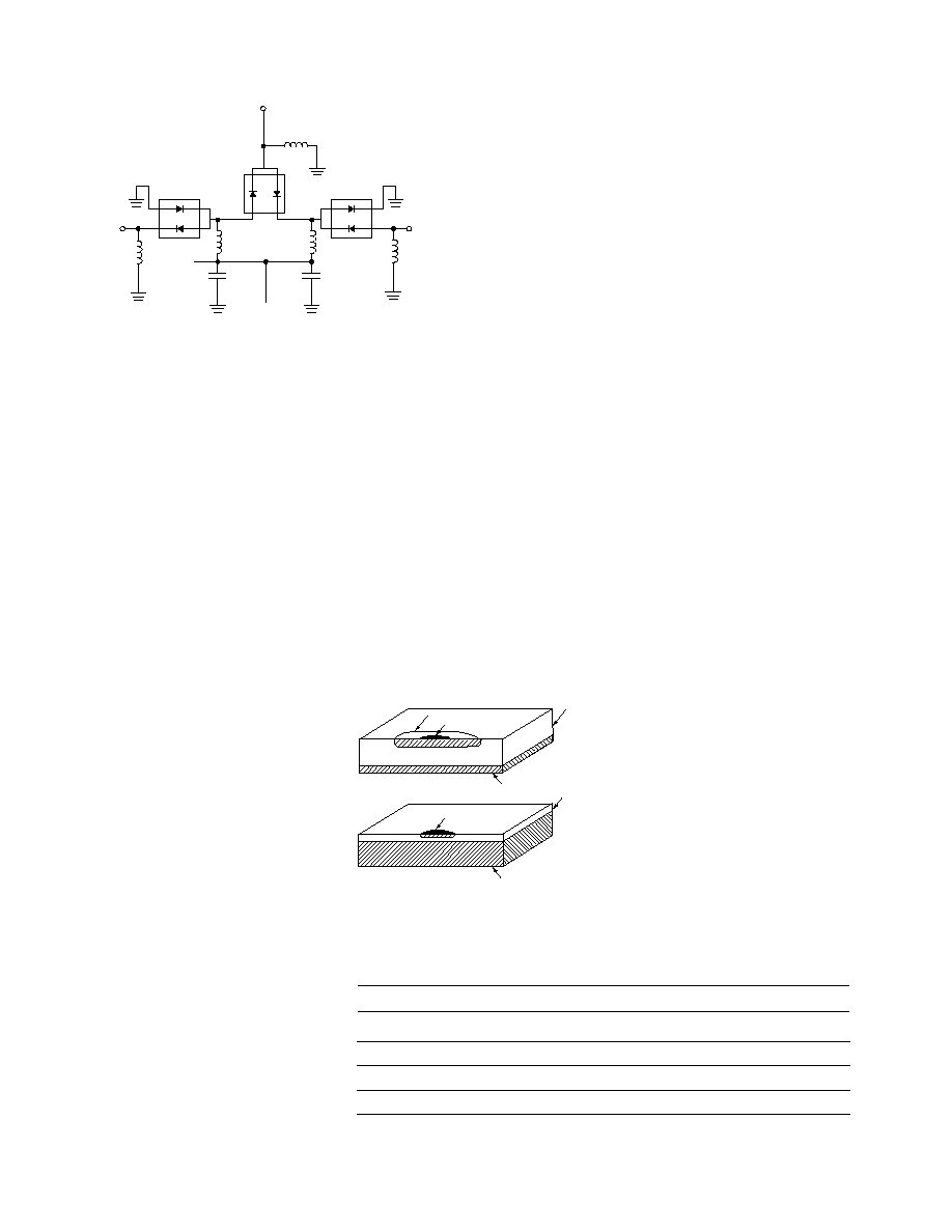
Typical Applications
RF COMMON
RF 1
1
2
3
4
BIAS 1
RF 2
BIAS 2
RF COMMON
RF 2
BIAS
RF 1
2
3
4
1
2
3
4
1
Figure 6. Simple SPDT Switch Using Only Positive Bias.
Figure 7. High Isolation SPDT Switch Using Dual Bias.
120
115
110
105
100
95
90
85
1
10
30
I
F
≠ FORWARD BIAS CURRENT (mA)
Figure 3. 2nd Harmonic Input Intercept Point
vs. Forward Bias Current.
INPUT INTERCEPT POINT (dBm)
Diode Mounted as a
Series Attenuator in a
50 Ohm Microstrip and
Tested at 123 MHz
0.50
0.45
0.40
0.35
0.30
0.25
0.20
0.15
0
4
8
12
16
20
V
R
≠ REVERSE VOLTAGE (V)
TOTAL CAPACITANCE (pF)
1 MHz
1 GHz
Figure 2. Capacitance vs. Reverse Voltage.
200
160
120
80
40
0
10
20
15
25
30
T
rr
≠
REVERSE RECOVERY TIME (nS)
FORWARD CURRENT (mA)
Figure 4. Typical Reverse Recovery Time vs.
Reverse Voltage.
V
R
= ≠2V
V
R
= ≠5V
V
R
= ≠10V
100
10
1
0.1
0.01
0
0.2
0.4
0.6
0.8
1.0
1.2
I
F
≠
FORWARD CURRENT (mA)
V
F
≠ FORWARD VOLTAGE (V)
Figure 5. Forward Current vs. Forward Voltage.
125
∞
C
25
∞
C ≠50
∞
C
Intercept point
will be higher
at higher
frequencies
Figure 1. Total RF Resistance at 25
∞
C vs.
Forward Bias Current.
10
1
RF RESISTANCE (OHMS)
I
F
≠ FORWARD BIAS CURRENT (mA)
0.1
1
10
100
4
Applications Information
PIN Diodes
In RF and microwave networks,
mechanical switches and attenua-
tors are bulky, often unreliable,
and difficult to manufacture.
Switch ICs, while convenient to
use and low in cost in small
quantities, suffer from poor
distortion performance and are
not as cost effective as PIN diode
switches and attenuators in very
large quantities. For over 30 years,
designers have looked to the PIN
diode for high performance/low
cost solutions to their switching
and level control needs.
In the RF and microwave ranges,
the switch serves the simple
purpose which is implied by its
name; it operates between one of
two modes, ON or OFF. In the ON
state, the switch is designed to
have the least possible loss. In the
OFF state, the switch must exhibit
a very high loss (isolation) to the
input signal, typically from 20 to
60 dB. The attenuator, however,
serves a more complex function.
It provides for the "soft" or
controlled variation in the power
level of a RF or microwave signal.
At the same time as it attenuates
the input signal to some predeter-
mined value, it must also present a
matched input impedance (low
VSWR) to the source. Every
microwave network which uses
PIN diodes (phase shifter, modula-
tor, etc.) is a variation on one of
these two basic circuits.
One can see that the switch and
the attenuator are quite different
in their function, and will there-
fore often require different
characteristics in their PIN diodes.
These properties are easily
controlled through the way in
which a PIN diode is fabricated.
See Figure 9.
Bulk Attenuator Diode
Epi Switching Diode
P+ Diffusion
Bulk
I-Layer
N+ Diffusion
Metal Contact
;
;
Contact Over
P+ Diffusion
N+ Substrate
Epi
I-Layer
Figure 9. PIN Diode Construction.
RF COMMON
RF 2
RF 1
BIAS
2
3
4
1
2
3
4
1
3
4
1
2
Figure 8. Very High Isolation SPDT Switch, Dual Bias.
Diode Construction
At Agilent Technologies, two basic
methods of diode fabrication are
used. In the case of bulk diodes, a
wafer of very pure (intrinsic)
silicon is heavily doped on the top
and bottom faces to form P and N
regions. The result is a diode with
a very thick, very pure I region.
The epitaxial layer (or EPI) diode
starts as a wafer of heavily doped
silicon (the P or N layer), onto
which a thin I layer is grown.
After the epitaxial growth, diffu-
sion is used to add a heavily doped
(N or P) layer on the top of the epi,
creating a diode with a very thin I
layer populated by a relatively
large number of imperfections.
These two different methods of
design result in two classes of
diode with distinctly different
characteristics, as shown in
Table 1.
As we shall see in the following
paragraphs, the bulk diode is
almost always used for attenuator
applications and sometimes as a
switch, while the epi diode (such
as the HMPP-3890) is generally
used as a switching element.
Diode Lifetime and Its Implications
The resistance of a PIN diode is
controlled by the conductivity (or
resistivity) of the I layer. This
conductivity is controlled by the
density of the cloud of carriers
(charges) in the I layer (which is, in
turn, controlled by the DC bias).
Minority carrier lifetime, indicated
by the Greek symbol
, is a
Table 1. Bulk and EPI Diode Characteristics.
Characteristic
EPI Diode
Bulk Diode
Lifetime
Short
Long
Distortion
High
Low
Current Required
Low
High
I Region Thickness
Very Thin
Thick

5
measure of the time it takes for the
charge stored in the I layer to
decay, when forward bias is
replaced with reverse bias, to some
predetermined value. This lifetime
can be short (35 to 200 nsec. for
epitaxial diodes) or it can be
relatively long (400 to 3000 nsec.
for bulk diodes). Lifetime has a
strong influence over a number of
PIN diode parameters, among
which are distortion and basic
diode behavior.
To study the effect of lifetime on
diode behavior, we first define a
cutoff frequency f
C
= 1/
. For short
lifetime diodes, this cutoff fre-
quency can be as high as 30 MHz
while for our longer lifetime
diodes f
C
400 KHz. At frequen-
cies which are ten times f
C
(or
more), a PIN diode does indeed
act like a current controlled
variable resistor. At frequencies
which are one tenth (or less) of f
C
,
a PIN diode acts like an ordinary
PN junction diode. Finally, at
0.1f
C
f
10f
C
, the behavior of the
diode is very complex. Suffice it to
mention that in this frequency
range, the diode can exhibit very
strong capacitive or inductive
reactance -- it will not behave at
all like a resistor. However, at zero
bias or under heavy forward bias,
all PIN diodes demonstrate very
high or very low impedance
(respectively) no matter what
their lifetime is.
Diode Resistance vs. Forward Bias
If we look at the typical curves for
resistance vs. forward current for
bulk and epi diodes (see Figure
10), we see that they are very
different. Of course, these curves
apply only at frequencies > 10 f
C
.
One can see that the curve of
resistance vs. bias current for the
bulk diode is much higher than
that for the epi (switching) diode.
Figure 11. Linear Equivalent Circuit of the
MiniPak PIN Diode.
Thus, for a given current and
junction capacitance, the epi
diode will always have a lower
resistance than the bulk diode.
The thin epi diode, with its
physically small I region, can
easily be saturated (taken to the
point of minimum resistance) with
very little current compared to the
much larger bulk diode. While an
epi diode is well saturated at
currents around 10 mA, the bulk
diode may require upwards of
100 mA or more. Moreover, epi
diodes can achieve reasonable
values of resistance at currents of
1 mA or less, making them ideal
for battery operated applications.
Having compared the two basic
types of PIN diode, we will now
focus on the HMPP-3890 epi
diode.
Given a thin epitaxial I region, the
diode designer can trade off the
device's total resistance (R
S
+ R
j
)
and junction capacitance (C
j
) by
varying the diameter of the
contact and I region. The
HMPP-3890 was designed with the
930 MHz cellular and RFID, the
1.8 GHz PCS and 2.45 GHz RFID
markets in mind. Combining the
low resistance shown in Figure 10
with a typical total capacitance of
0.27 pF, it forms the basis for high
performance, low cost switching
networks.
1000
100
10
1
RESISTANCE (
)
BIAS CURRENT (mA)
0.01
0.1
1
10
100
HMPP-389x
Epi PIN Diode
HSMP-3880 Bulk PIN Diode
Figure 10. Resistance vs, Forward Bias.
Linear Equivalent Circuit
In order to predict the perfor-
mance of the HMPP-3890 as a
switch, it is necessary to construct
a model which can then be used in
one of the several linear analysis
programs presently on the market.
Such a model is given in Figure 11,
where R
S
+ R
j
is given in Figure 1
and C
j
is provided in Figure 2.
Careful examination of Figure 11
will reveal the fact that the
package parasitics (inductance
and capacitance) are much lower
for the MiniPak than they are for
leaded plastic packages such as
the SOT-23, SOT-323 or others.
This will permit the HMPP-389x
family to be used at higher fre-
quencies than its conventional
leaded counterparts.
30 fF
30 fF
20 fF
20 fF
1.1 nH
Single diode package (HMPP-3890)
2
3
1
4
30 fF
30 fF
20 fF
20 fF
12 fF
12 fF
0.5 nH
Anti-parallel diode package (HMPP-3892)
2
3
1
4
0.5 nH
0.05 nH
0.5 nH
0.05 nH
0.05 nH
0.5 nH
0.05 nH
30 fF
30 fF
20 fF
20 fF
0.5 nH
0.05 nH
Parallel diode package (HMPP-3895)
2
3
1
4
0.5 nH
0.05 nH
0.5 nH
0.05 nH
0.5 nH
0.05 nH