Agilent Tachyon DX4+ (HPFC-5700)
Dual-Channel 4-Gb Fibre Channel Controller
With The Data Integrity Field (DIF) Feature
Preliminary Product Overview
Eight GPIO pins per channel
W
Product Description
The Tachyon DX4+ is a high-
performance PCI/PCI-X native
dual Channel controller, that
supports 4/2/1 Gb/s data transfer
rates for host bus adapters and
embedded sub-systems. DX4+ is
the sixth generation member of
the Agilent Technologies family of
Fibre Channel interface
controllers.
It provides the performance
enhancing features of PCI-X and
is a single chip solution that
offers the most economical
component cost savings. The
DX4+ interfaces directly to an
industry standard PCI/PCI-X bus
and includes an internal SERDES
capable of supporting 4/2/1 Gb/s
data rates.
The DX4+ Data Integrity Field
(DIF) is an Agilent industry-
leading feature. It provides a
robust CRC-based data protection
scheme with mechanisms to
initiate, extend or terminate a
protection domain, which can
span both the PCI interface as
well as the Fibre Channel
interface. When combined with
Fibre Channel's standard CRC,
DIF offers complete data
protection in the I/O data path.
DIF is performed in State-
Machine hardware to maximize
performance. (Agilent's DIF
feature is a subset of an industry
standard "End to End" data
integrity proposal that is
currently being proposed and
discussed in the SCSI T-10
standards forum.)
Applications
∑Embedded Subsystems
∑Disk Arrays
∑SCSI Bridge
∑High-performance Host Bus
Adapters
Features
Dual channel Fibre Channel
operation on one chip for the
lowest overall FC solution costs
Full duplex operation for each
channel
Concurrent channel operation at
full link rate
4, 2 and 1 Gb Fibre Channel
operation support via internal
transceivers
Dual function industry standard
66 MHz PCI or 66/100/133 MHz
PCI-X backplane interface with
32/64 bit support
3.3V PCI/PCI-X I/O
Compliance to PCI Local Bus
Specification, Rev 2.2
MSI (Message Signaled Interrupt)
support
Compliance to PCI-X Addendum,
Rev 1.0A
PCI/PCI-X hot plug compatible
Output impedance control on PCI-X
I/O for point-to-point or multi-
point connectivity
Loss of signal indication (per
channel) during internal SERDES
mode
Multiple split read transaction
support on PCI-X
No external SRAM required for
operation
4K on-chip boot RAM
Supports fabric, point-to-point
(N_Port) and loop (Public and
Private) topologies
Virtual N_Port I.D
Optional external boot ROM/Flash
(128K Bytes)
Eight full-frame inbound buffers
and four full-frame outbound
buffers per channel
State machine processing of
inbound and outbound data
Fully assisted Class 2 and Class 3
FCP with simultaneous initiator
and target functionality
Full byte-level parity protection on
internal data path and RAM
Backwards compatible to Tachyon
XL2 and DX2 programming
interface
Supports ACK_0 and ACK_1
models in hardware
Complete sequence segmentation
and reassembly done in hardware
64-bit addressing (44/45 bits per
Length/Address pair)
Mechanisms to reduce number of
interrupts generated by the adapter
help reduce the software overhead
required to support the adapter
Frame payload size up to 2048
bytes
Loop map, broadcast, directed
reset and bypass support
Non-zero login BB_Credit support
Compliance with FC-AL-2 ANSI
Standard
Compliance with Hardware Design
Guide for Microsoft Windows NT
Server, Version 2.0
Compatible with ACPI/Power
Management Specification
Minimal board space required
Support of the No Snoop feature in
PCI/X mode for performance
improvement in software-based
cache-coherent systems
Preliminary Product Disclaimer
This preliminary product information is provided to assist you in the evaluation of product(s) currently under development. Until Agilent Technologies releases this
product for general sale, Agilent Technologies reserves the right to alter prices, specifications, features, capabilities, functions, release dates, and general availability
of the product(s) at anytime.
Tachyon DX4+ Architecture
The Tachyon DX4+ is compatible
with previous Tachyon XL2 and
DX2 products, enabling
customers to leverage existing
firmware and software.
The DX4+ architecture has
numerous independent functional
blocks which concurrently
process inbound data, outbound
data, control and commands in
hardware. This results in the
lowest latency and highest
performance in a multi-function
device.
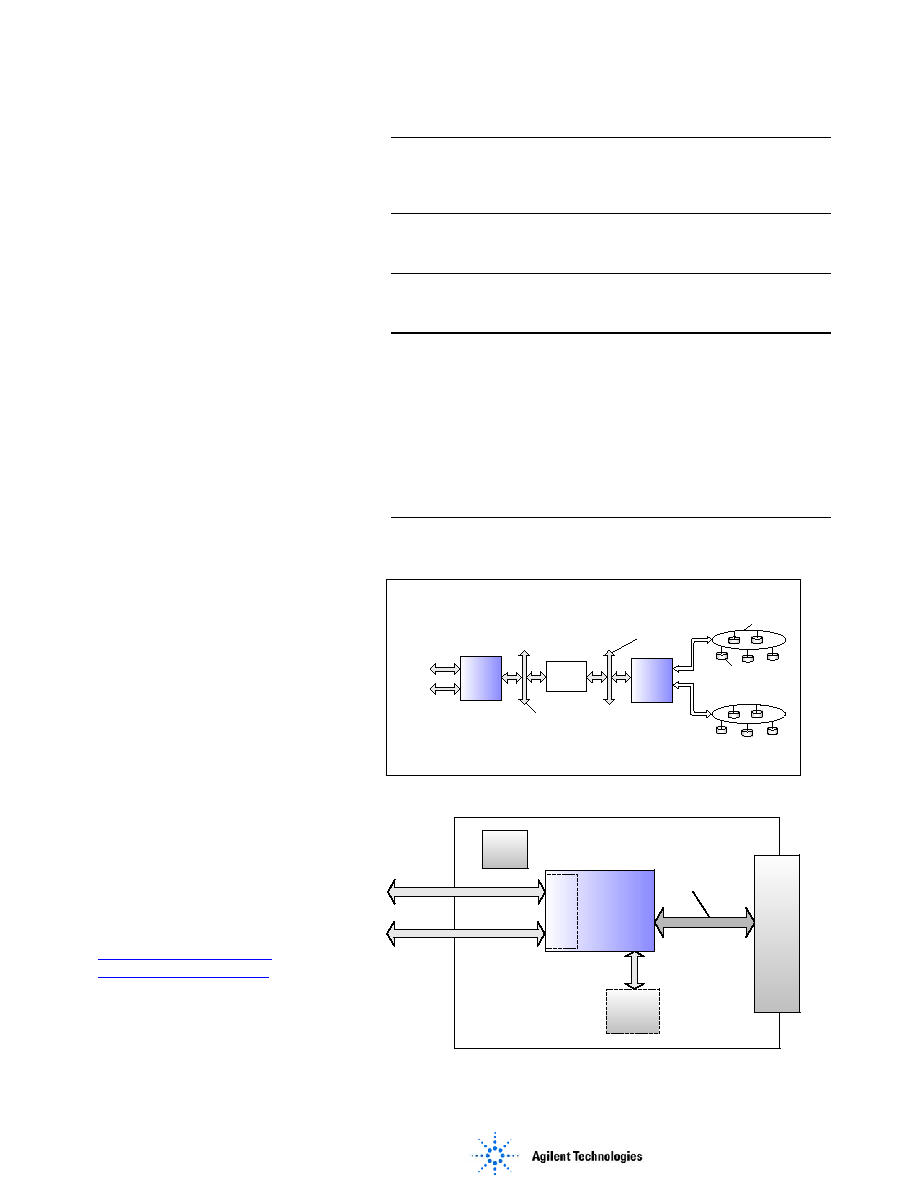
Typical Subsystem Application
Figure 1 shows DX4+ in an
optional high-performance
configuration.
The DX4+ chips interface between
the mass storage devices on the
Fibre Channel loops, the main
memory of the subsystem and the
host.
In this example, the DX4+ chips
interface with main memory
cache through 66 MHz PCI or
66/100/133 MHz PCI-X backplane,
with 32/64-bit support in either
mode.
Host Bus Adapter Example
Figure 2 shows an example of a
DX4+ on a generic host bus
adapter.
On the backplane, the DX4+ inter-
faces directly to an industry
standard 66 MHz PCI or
66/100/133 MHz PCI-X bus.
The onboard optional boot
ROM/Flash ROM is connected
directly to the DX4+ chip.
Additional Features
Figure 1
Figure 2
DIF provides a mechanism for initiating, extending and
terminating robust data protection domains
Standard Fibre Channel CRC support
Full byte-level parity protection on data path
Data Integrity Features
Enables leverage across future 4 and 10 Gb products
Preliminary Specifications
Package Type: FC PBGA, 1mm ball pitch
Power Dissipation: ~ 3.5 Watts
Thermal Specification: 0 - 110∞C, T
Junction
Voltage Margin: ± 5%
Registers memory mapped
Maintain Tachyon Fibre
Channel Family
Programming Model
(Similar to DX2+)
Backward compatible offsets for Fibre Channel core registers
Performance scalable State Machine-based architecture
Independent, concurrent inbound/outbound transaction
processing
Multiple outbound context support
Support for SCSI initiator, target and initiator/target modes
Complete sequence segmentation and reassembly done in
hardware
Up to 2048-byte frame payloads
Fully assisted FC-FS Class 2 and Class 3 support
ACK0/ACK1 models in hardware
Interrupt avoidance mechanisms
Standard Tachyon Fibre
Channel Core Feature Set
64-bit addressing (44/45 bits per Length/Address pair)
FC Link
FC Link
32-Bit/64-Bit PCI
(66 MHz)
or
32-Bit/64-Bit PCI-X
(66-133 MHz)
32-Bit/64-Bit PCI
(66 MHz)
or
32-Bit/64-Bit PCI-X
(66-133 MHz)
FC Loop
Mass Storage Device
Main
Memory
Cache
DX4+
DX4+
Flash
ROM
B
a
ckpl
ane
C
onnector
FC Link # 2
32-Bit/64-Bit PCI
(66 MHz)
or
32-Bit/64-Bit PCI-X
(66-133 MHz)
Clock
DX4+
Int
egrat
e
d
Transc
e
iv
er
FC Link # 1
For product information please go to our web sites.
www.semiconductor.agilent.com
www.agilent.com/view/storage
Copyright © 2004 Agilent Technologies Inc.
March 17, 2004
Preliminary Product Disclaimer
This preliminary product information is provided to assist you in the evaluation of product(s) currently under development. Until Agilent Technologies releases this
product for general sale, Agilent Technologies reserves the right to alter prices, specifications, features, capabilities, functions, release dates, and general availability
of the product(s) at anytime.